 |
NEXT-STATE TABLE: Flip-flop Transition Table, Karnaugh Maps |
| << DIGITAL CLOCK: Clocked Synchronous State Machines |
| D FLIP-FLOP BASED IMPLEMENTATION >> |
CS302 -
Digital Logic & Design
Lesson
No. 31
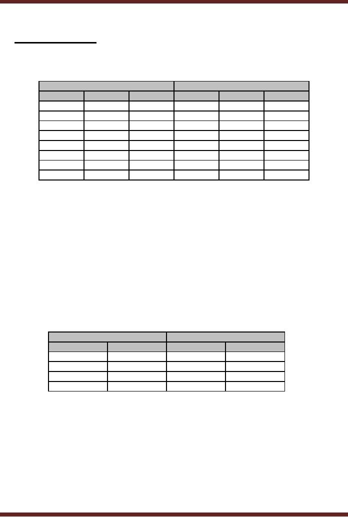
2. NEXT-STATE
TABLE
Once
the state diagram of the
sequential circuit is defined, a
Next-State Table is
derived
which lists each present
state and the corresponding
next state. The next
state is the
state to
which the sequential circuit
switches when a clock
transition occurs. Table
31.1
Present
State
Next
State
Q2
Q1
Q0
Q2
Q1
Q0
0
0
0
0
0
1
0
0
1
0
1
0
0
1
0
0
1
1
0
1
1
1
0
0
1
0
0
1
0
1
1
0
1
1
1
0
1
1
0
1
1
1
1
1
1
0
0
0
Table
31.1
Next-State
Table for a 3-bit
Up-Counter
3. Flip-flop
Transition Table
The
Memory element of the
Sequential circuit is implemented
using flip-flops. The
number of
flip-flops used is determined by
the total number of states.
When there is a clock
transition at
the clock input of the
flip-flops they change from
their present state to the
next
state.
The Flip-flop transition
table lists all the
possible flip-flop input
combinations which
allow
the
present state to change to
the next state on a clock
transition. The flip-flop
transition table
is based on
the flip-flop used (D,
S-R or J-K). Table 31.2. In
the transition table the
present
state
logic 0 changes to next
state logic 0, when J-K
inputs are 0 and 0
respectively or J-K
inputs
are 0 and 1 respectively.
Thus if input J=0 the
next state output is 0.
Similarly when J-K
inputs
are 1 and 1 or 1 and 0 the
next state output is set to
logic 1. Thus if input J=1
the next
state
output is 1. Similarly for
the other two transition
cases K=1 and K=0
sets the next
state
output to
logic 0 and 1
respectively.
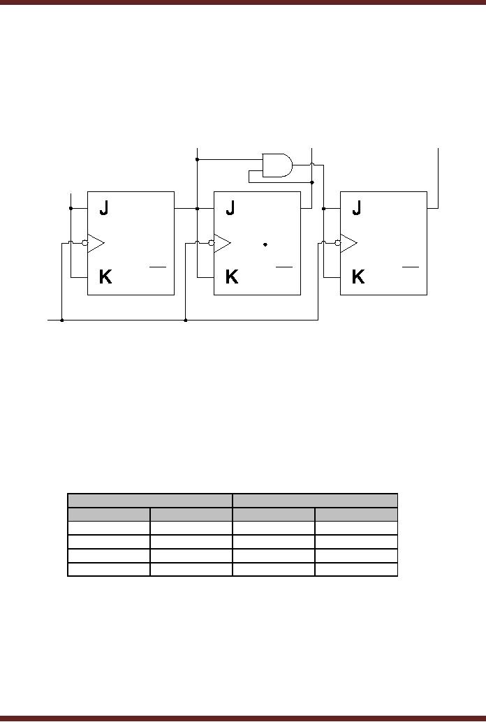
Flip-flop
Inputs
Output
Transitions
J
K
Qt
Qt+1
0
x
0
0
1
x
0
1
x
1
1
0
x
0
1
1
Table
31.2
J-K
flip-flop Transition
table
4. Karnaugh
Maps
For
each state variable shown in
the Next-State table, the
change from present state
to
the
next state on a clock
transition depends upon the
J-K inputs. Table 31.3.
Considering the
state
variable Q2, J2 and K2
inputs
set to 0 and x (don't care)
allow Q2
to change
from present
state 0 to
next state 0. Similarly, the
state variable Q0 changes from 1 to 0 when
J0 and K0
inputs
are set at x (don't care)
and 1 respectively. The
table is completed using the
information
321
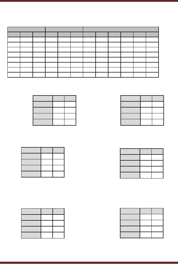
CS302 -
Digital Logic & Design
in the
Next-State table and the
J-K flip-flop transition
table. The J-K inputs
can be directly
mapped to
Karnaugh maps. Table
31.4
Present
State
Next
State
J-K
flip-flop inputs
Q2
Q1
Q0
Q2
Q1
Q0
J2
K2
J1
K1
J0
K0
0
0
0
0
0
1
0
x
0
x
1
x
0
0
1
0
1
0
0
x
1
x
x
1
0
1
0
0
1
1
0
x
x
0
1
x
0
1
1
1
0
0
1
x
x
1
x
1
1
0
0
1
0
1
x
0
0
x
1
x
1
0
1
1
1
0
x
0
1
x
x
1
1
1
0
1
1
1
x
0
x
0
1
x
1
1
1
0
0
0
x
1
x
1
x
1
Table
31.3
J-K
flip-flop input table
Q2Q1/Q0
0
1
Q2Q1/Q0
0
1
00
0
0
00
x
x
01
0
1
01
x
x
11
x
x
11
0
1
10
x
x
10
0
0
J2 = Q1Q 0
K 2 = Q1Q 0
Table
31.4a
Karnaugh Map
for J2 and K2 inputs
Q2Q1/Q0
0
1
Q2Q1/Q0
0
1
00
0
1
00
x
x
01
x
X
01
0
1
11
x
X
11
0
1
10
0
1
10
x
x
J1 = Q 0
K1 = Q0
Table
31.4b
Karnaugh Map
for J1 and K1 inputs
Q2Q1/Q0
0
1
Q2Q1/Q0
0
1
00
x
1
00
1
x
01
x
1
01
1
x
11
x
1
11
1
x
10
x
1
10
1
x
J0 = 1
K0 = 1
Table
31.4c
Karnaugh Map
for J0 and K0 inputs
322
CS302 -
Digital Logic & Design
5. Logic
expressions for Flip-flop
Inputs
Simplified
expressions for J2-K2, J1-K1 and
J0-K0 are
directly obtained from
the
Karnaugh
maps. The expressions are
shown along with the
Karnaugh maps.
6. Sequential
Circuit Implementation
The
Boolean expressions obtained in
the previous step are
implemented using
logic
gates.
The sequential circuit
implemented is shown in figure
30.8.
Q0
Q1
Q2
1
SET
SET
SET
Q
Q
Q
flip-flop
1
flip-flop
2
flip-flop
3
Q
Q
Q
CLR
CLR
CLR
CLK
Figure
31.1
Implementation
of the Sequential
Circuit
The
3-bit up counter can be
implemented using S-R
flip-flops and D
flip-flops.
Implementation
of the counter using S-R
flip-flop requires the use
of S-R flip-flop
transition
table in
step 3. The remaining steps
follow step 3.
S-R
flip-flop based
Implementation
Flip-Flop
Transition Table
To implement
the counter using S-R
flip-flops instead of J-K
flip-flops, the S-R
transition
table is used. The S-R
flip-flop does not allow S
and R inputs to be set to
logic 1 and
1 respectively
and is considered to be an invalid
state. Based on the three
set of valid inputs
the
S-R transition table is
shown. Table 31.5
Flip-flop
Inputs
Output
Transitions
S
R
Qt
Qt+1
0
x
0
0
1
0
0
1
0
1
1
0
x
0
1
1
Table
31.5
S-R
flip-flop Transition
table
Karnaugh
Maps
The
S-R input table is shown in
table 31.6. The Karnaugh
maps for the
input
expressions
are also derived from
the input table.
323
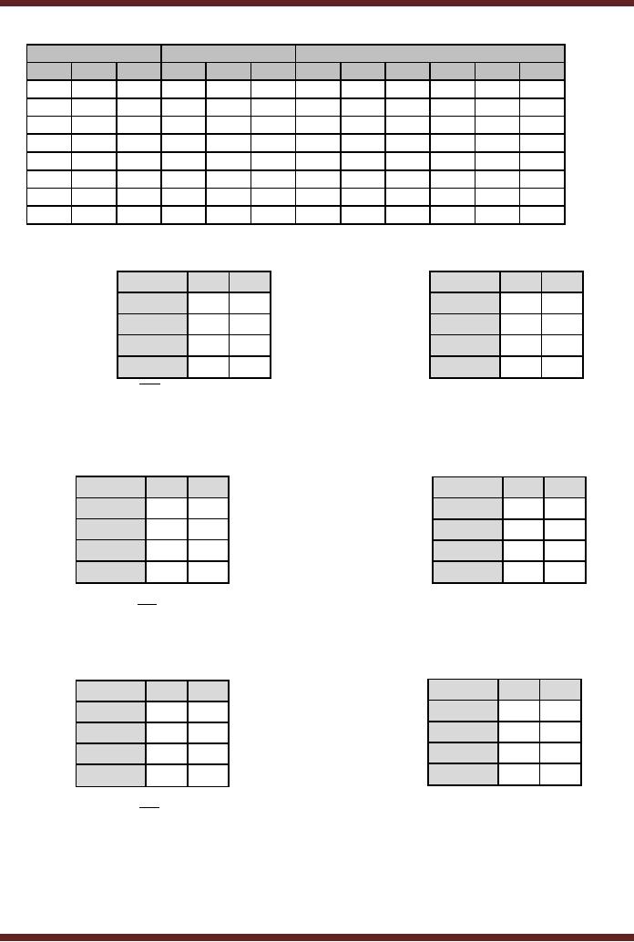
CS302 -
Digital Logic & Design
Present
State
Next
State
S-R
flip-flop inputs
Q2
Q1
Q0
Q2
Q1
Q0
S2
R2
S1
R1
S0
R0
0
0
0
0
0
1
0
x
0
x
1
0
0
0
1
0
1
0
0
x
1
0
0
1
0
1
0
0
1
1
0
x
x
0
1
0
0
1
1
1
0
0
1
0
0
1
0
1
1
0
0
1
0
1
x
0
0
x
1
0
1
0
1
1
1
0
x
0
1
0
0
1
1
1
0
1
1
1
x
0
x
0
1
0
1
1
1
0
0
0
0
1
0
1
0
1
Table
31.6
S-R
flip-flop input table
Q2Q1/Q0
0
1
Q2Q1/Q0
0
1
00
0
0
00
x
x
01
0
1
01
x
0
11
x
0
11
0
1
10
x
x
10
0
0
S 2 = Q 2Q1Q 0
R 2 = Q 2Q1Q 0
Table
31.7a
Karnaugh Map
for S2 and R2 inputs
Q2Q1/Q0
0
1
Q2Q1/Q0
0
1
00
0
1
00
x
0
01
x
0
01
0
1
11
x
0
11
0
1
10
0
1
10
x
0
R1 = Q1Q 0
S1 = Q1Q 0
Table
31.7b
Karnaugh Map
for S1 and R1 inputs
Q2Q1/Q0
0
1
Q2Q1/Q0
0
1
00
0
1
00
1
0
01
0
1
01
1
0
11
0
1
11
1
0
10
0
1
10
1
0
S0 = Q0
R0 = Q0
Karnaugh Map
for S0 and R0 inputs
Table
31.7c
Logic
expressions for Flip-flop
Inputs
324
CS302 -
Digital Logic & Design
Simplified
expressions for S2-R2, S1-R1 and
S0-R0 are
directly obtained from
the
Karnaugh
maps. The expressions are
shown along with the
Karnaugh maps.
Sequential
Circuit Implementation
The
implementation of the 3-bit
synchronous counter based on
S-R flip-flops is
shown.
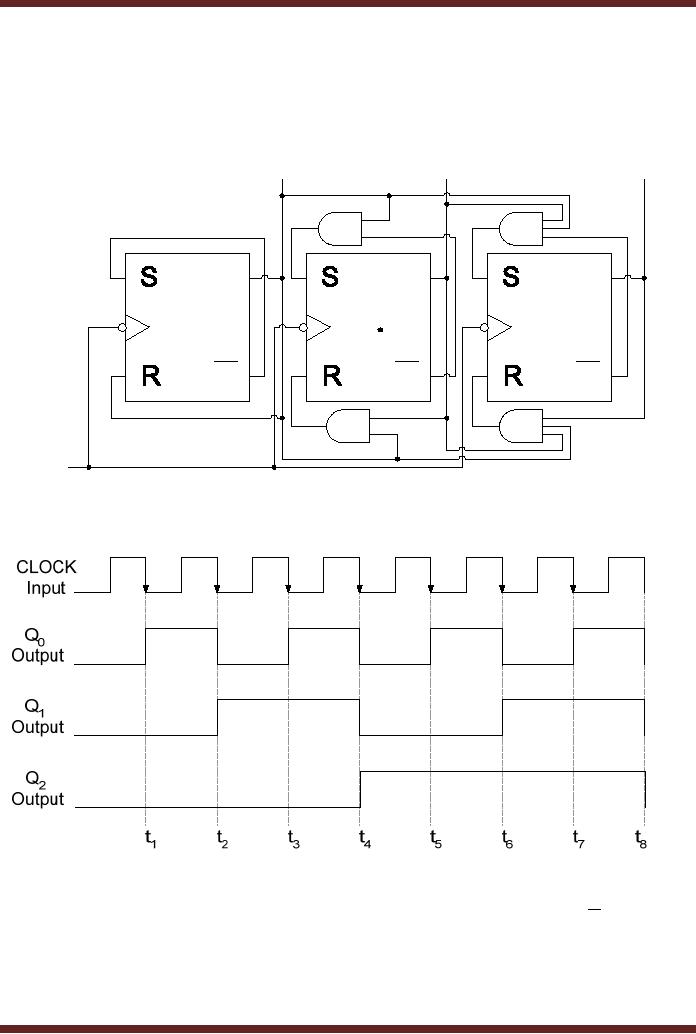
Figure
31.2
Q0
Q1
Q2
SET
SET
SET
Q
Q
Q
flip-flop
1
flip-flop
2
flip-flop
3
Q
Q
Q
CLR
CLR
CLR
CLK
Figure
31.2a S-R flip-flop based
implementation of 3-bit Synchronous
Counter
Figure
31.2b Timing diagram of the
S-R flip-flop based 3-bit
Synchronous Counter
The
S-R inputs of the first
flip-flop are cross
connected to its Q and Q outputs.
At
interval
t1 the Q0 output is at logic 0, the R
input is at logic 0 and S
input is at logic 1, thus
the
flip-flop is
set to logic 1. When the
Q0 output is at logic
1, the S and R inputs are at
logic 0 and
1 respectively,
thus at t2
the
clock transition the
flip-flop is reset to 0. At t1 the S and R inputs
of
the
second-flip-flop are at logic 0 as
Q0 is at logic 0,
thus at the clock transition
the output of
325

CS302 -
Digital Logic & Design
the
second flip-flop remains
unchanged. At interval t2, the S and R inputs of
the second flip-
flop
are set to 1 and 0
respectively, thus it is set to
logic 1 on the clock
transition. Similarly, at
interval
t4 the S-R
inputs of the third
flip-flop are set to logic 1
and 0 respectively, the
flip-flop is
set to
logic 1 on the clock
transition.
326
Table of Contents:
- AN OVERVIEW & NUMBER SYSTEMS
- Binary to Decimal to Binary conversion, Binary Arithmetic, 1s & 2s complement
- Range of Numbers and Overflow, Floating-Point, Hexadecimal Numbers
- Octal Numbers, Octal to Binary Decimal to Octal Conversion
- LOGIC GATES: AND Gate, OR Gate, NOT Gate, NAND Gate
- AND OR NAND XOR XNOR Gate Implementation and Applications
- DC Supply Voltage, TTL Logic Levels, Noise Margin, Power Dissipation
- Boolean Addition, Multiplication, Commutative Law, Associative Law, Distributive Law, Demorgans Theorems
- Simplification of Boolean Expression, Standard POS form, Minterms and Maxterms
- KARNAUGH MAP, Mapping a non-standard SOP Expression
- Converting between POS and SOP using the K-map
- COMPARATOR: Quine-McCluskey Simplification Method
- ODD-PRIME NUMBER DETECTOR, Combinational Circuit Implementation
- IMPLEMENTATION OF AN ODD-PARITY GENERATOR CIRCUIT
- BCD ADDER: 2-digit BCD Adder, A 4-bit Adder Subtracter Unit
- 16-BIT ALU, MSI 4-bit Comparator, Decoders
- BCD to 7-Segment Decoder, Decimal-to-BCD Encoder
- 2-INPUT 4-BIT MULTIPLEXER, 8, 16-Input Multiplexer, Logic Function Generator
- Applications of Demultiplexer, PROM, PLA, PAL, GAL
- OLMC Combinational Mode, Tri-State Buffers, The GAL16V8, Introduction to ABEL
- OLMC for GAL16V8, Tri-state Buffer and OLMC output pin
- Implementation of Quad MUX, Latches and Flip-Flops
- APPLICATION OF S-R LATCH, Edge-Triggered D Flip-Flop, J-K Flip-flop
- Data Storage using D-flip-flop, Synchronizing Asynchronous inputs using D flip-flop
- Dual Positive-Edge triggered D flip-flop, J-K flip-flop, Master-Slave Flip-Flops
- THE 555 TIMER: Race Conditions, Asynchronous, Ripple Counters
- Down Counter with truncated sequence, 4-bit Synchronous Decade Counter
- Mod-n Synchronous Counter, Cascading Counters, Up-Down Counter
- Integrated Circuit Up Down Decade Counter Design and Applications
- DIGITAL CLOCK: Clocked Synchronous State Machines
- NEXT-STATE TABLE: Flip-flop Transition Table, Karnaugh Maps
- D FLIP-FLOP BASED IMPLEMENTATION
- Moore Machine State Diagram, Mealy Machine State Diagram, Karnaugh Maps
- SHIFT REGISTERS: Serial In/Shift Left,Right/Serial Out Operation
- APPLICATIONS OF SHIFT REGISTERS: Serial-to-Parallel Converter
- Elevator Control System: Elevator State Diagram, State Table, Input and Output Signals, Input Latches
- Traffic Signal Control System: Switching of Traffic Lights, Inputs and Outputs, State Machine
- Traffic Signal Control System: EQUATION DEFINITION
- Memory Organization, Capacity, Density, Signals and Basic Operations, Read, Write, Address, data Signals
- Memory Read, Write Cycle, Synchronous Burst SRAM, Dynamic RAM
- Burst, Distributed Refresh, Types of DRAMs, ROM Read-Only Memory, Mask ROM
- First In-First Out (FIFO) Memory
- LAST IN-FIRST OUT (LIFO) MEMORY
- THE LOGIC BLOCK: Analogue to Digital Conversion, Logic Element, Look-Up Table
- SUCCESSIVE APPROXIMATION ANALOGUE TO DIGITAL CONVERTER