 |
Advanced Computer
Architecture-CS501
________________________________________________________
Advanced
Computer Architecture
Lecture
No. 24
Reading
Material
Handouts
Slides
Summary
·
Designing
Parallel I/O Ports
·
Practical
Implementation of the
SAD
·
NUXI
Problem
·
Variation
in the Implementation of the Address
Decoder
·
Estimating
the Delay Interval
Designing
Parallel I/O Ports
This
section is about designing
parallel input and output
ports. As you already
know
from
the previous discussion, an
interface that is used to
connect the computer bus
with
I/O devices is
called an I/O port. This I/O
port can be connected directly to
the computer
bus (also
called the system bus) or
through an intermediate bus called
the I/O bus. This
intermediate
bus is also called the expansion bus or
the peripheral bus. In any
case, the
following
general information about I/O bus
cycles on a typical CPU
should be kept in
mind: At
the start of a particular bus
cycle (which will be an I/O bus cycle in
this case),
the
CPU places an address on its
address bus. This address
will identify the I/O device
to
be
involved in the transfer.
After some time the
CPU will activate certain
control signals,
which
will indicate whether the
particular I/O bus cycle, is an I/O read
or an I/O write
cycle.
Based on these control
signals, in case of I/O read
cycle, the CPU will
be
expecting
data from the selected
input device over the
data bus, and for an I/O
write cycle
the
CPU will provide data to the
selected device over the
data bus. At the end of this
I/O
bus
cycle, the address (and
data) information will be removed from
the buses and the
control
signals will be reset. It can be easily
understood from this
discussion that we
must
match the timing
requirements of the I/O ports to be
designed with the
timing
parameters
of the given CPU.
Additionally, the voltage and
current requirements of
the
I/O ports
must be matched with the
voltage and current specifications of
the CPU. For
simplicity,
we ignore the voltage and
current matching details in
this discussion and
only
focus on
the logic levels and timing
aspects of the design. Voltage and
current related
discussions
are the topic of an
electronics course.
Thus,
there are two important
functions which should be
built into I/O ports.
1. Address
decoding
2. Data
isolation for input ports or
data capturing for output
ports.
Page
245
Last
Modified: 01-Nov-06
Advanced Computer
Architecture-CS501
________________________________________________________
1.
Address decoding: Since
every I/O port has a unique
identifier associated with
it,
(which is
called its address, and no
other port in the system
should have the
same
address),
by monitoring the system
address bus, the I/O port
knows when it is its turn
to
participate
in a transfer. At this time,
the address decoder within
the I/O port
generates
an
asserted output which can be
applied to the enable input of
tri-state buffers in
input
ports or
the latch enable input of
latches in output
ports.
Our
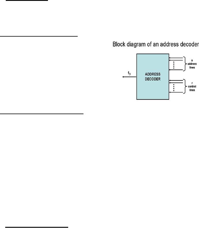
definition of an address decoder:
An
"Address Decoder" is a combinational
(logic)
circuit
with n + r
inputs
and a single output,
where
n
=
the number of address lines
into the
decoder,
and
r
=
the number of control lines
into the
decoder.
The
output fD is
active only when
the
corresponding
address is present on the n
address
lines and
the corresponding r
control
lines hold
the
"proper" (active or inactive)
value. fD
is
inactive
for all other
situations.
Suggestions
for address decoder
design:
1.1
Start by thinking of the
address decoder as a
"big AND
gate". We will call this a
"skeleton
address
decoder" or SAD. The output
of the SAD will be active
only when the
correct
address
is present on the system address bus and
the relevant control bus
signals hold the
proper
values. At all other times,
the output of the SAD
should be deactivated.
1.2
Always write the port
address of the port to be
designed in binary. Associate
the
CPU's
address lines with each
bit. Those lines which
are zero will be inverted
before
being
fed into the "big AND
gate"; other address lines
will not be inverted.
1.3
List the relevant control
signals for the system to
which the port is to be attached.
If
the
"proper" value of the signal
is 0, it should be inverted before
applying to the SAD,
otherwise
it is fed directly into the
SAD.
1.4
Determine whether the
decoder output should be
active high or low. This
will depend
on the
type of latch or buffer used
in the design. If an active low
decoder output is
needed,
invert the output from
the "big AND gate".
1.5
Once the logic for
the address decoder is established,
the SAD can be
implemented
using
any of the available methods
of logic design. For example, HDL
code in Verilog or
VHDL can be
generated and the address
decoder can be implemented using
PLDs.
Alternately,
the SAD can be implemented
using SSI building
blocks.
2.
Data isolation or capturing: For
input ports, the in coming
data should be placed on
the
data bus only during the I/O
read bus cycle. At all other
times, this data should
be
isolated
from the data bus otherwise
it will cause "bus contention".
Tri-state buffers are
used
for this purpose. Their
input lines are connected to
the peripheral device
supplying
data and
their output lines are
connected to the data bus.
The common enable line of
such
Page
246
Last
Modified: 01-Nov-06
Advanced Computer
Architecture-CS501
________________________________________________________
buffers
is driven with the output of
the SAD. If this enable is
active low, the output of
the
big AND
gate in the SAD should be
inverted, as described
earlier.
For
output ports, data is made
available for the peripheral
device at the data bus
during
the I/O
write bus cycle. During
other bus cycles, this data
will be removed from the
data
bus by
the processor. Latches (or
registers) are used for
this purpose. Their input
lines are
connected
to the system data bus and
their output lines are
connected to the
peripheral
device
receiving data. The common
clock (or latch enable)
line of such latches is
driven
with
the output of the SAD. If
this clock is active low,
the output of the big AND
gate in
the
SAD should be
inverted.
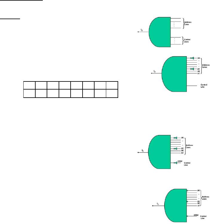
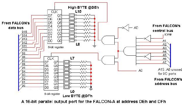
Example
# 1
Problem
Statement:
Design a
16-bit parallel output port
mapped on address DEh of the
I/O space of the
FALCON-A
CPU.
Solution:
Using
the guidelines mentioned above, we
start with a
"big AND
gate" (SAD) and write the
address to be
decoded
(DEh) in binary.
Thus,
DEh → 1101 1110 b.
Associating one CPU
address
line
with each bit, we get A0 = 0,
A1=1, etc as shown in
the
table below.
Because
the I/O space on the
FALCON-A is only 256
bytes,
address lines A15 .. A8 are
don't cares, and will not
be
used in
this design.
1
1
0
1
1
1
1
0
A7 A6 A5 A4 A3 A2
A1 A0
Thus, A0
and A5 will be applied to the "big AND
gate" after inversion. The
remaining
address
lines will be connected directly to
the inputs of the
SAD.
Next, we
look at the relevant control
signals. The only signal
which should be used in
this
case is
IOW#. A logic 0 (zero) on
this line indicates
that
it is
active. Thus, it should be
inverted before being
applied
to the input of the
SAD.
We can
easily see that our
SAD intuitively conforms
to
the
way we defined an address decoder.
Its output is a 1
only
when the address (xxxx xxxx 1101 1110 b)
is
present on
the FALCON-A's address bus
during an I/O
write
cycle (By the way,
this will take place when
the
instruction
out
reg, addr with
addr=DEh
or 222d is
executing
on the FALCON-A). At all
other times, its output
will
be
inactive.
To make
things simple, we use a
circle (or a bubble) to
indicate
an
inverter, as shown .Since
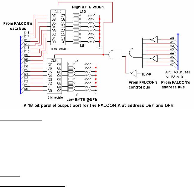
this is a 16-bit output
port, we will
use
two 8-bit registers to capture
data from the
FALCON-A's
data
bus. The output of the
SAD will be connected to the
enable
Page
247
Last
Modified: 01-Nov-06
Advanced Computer
Architecture-CS501
________________________________________________________
inputs of
the two registers. The
D-inputs of the registers will be
connected to the data
bus
and the Q
outputs of the registers will be
connected to the peripheral
device.
Practical
implementation of the SAD
Our
SAD in this design is an AND gate
with 9 inputs. Using SSI
chips, we can
implement
this SAD using an 8-input
AND gate and a 2-input AND gate as
shown in the
figure
shown below.
Displaying
output data using LED
branches:
An "LED
branch" is a combination of a resistor
and a light emitting diode (LED)
in
series.
Sixteen LED branches can be used to
display the output data
captured by the
registers as
shown in the figure
below.
Example
# 2
Problem
statement:
Given a
16-bit parallel output port
attached with the FALCON-A
CPU as shown in the
figure.
The port is mapped onto
address DEh of the
FALCON-A's I/O space.
Sixteen
LED
branches are used to display
the data being received
from the FALCON-A's
data
bus.
Every LED branch is wired in
such a way that when a 1
appears on the
particular
data bus
bit, it turns the LED
on; a 0 turns it off.
Which
LEDs will be ON when the
instruction
out
r2, 222 13
executes on
the CPU? Assume r2 contains
1234h.
Solution:
13
Depending
on the way the assembler is
written, the syntax of the
out
instruction
may allow only
the
decimal
form of the port address, or
only the hexadecimal form,
or both. Our version of the
assembler for
the
FALCON-A allows the decimal
form only. It also requires
that the port address be
aligned on 16-bit
"word
boundaries", which means
that every port address
should be divisible by 2.
Page
248
Last
Modified: 01-Nov-06
Advanced Computer
Architecture-CS501
________________________________________________________
Since r2
contains 1234h, the bit
pattern corresponding to this
value will be sent out to
the
output
port at address 222 (or
DEh). This is the address of
the output port in
this
example.
Writing the bit pattern in
binary will help us determine
the LEDs which will
be
ON.
Now
1234h gives us the following
bit associations with the
data bus
0
0
0
1
0
0
1
0
0
0
1
1
0
1
0
0
D15
D14 D13 D12 D11
D10 D9 D8 D7 D6 D5 D4 D3 D2 D1 D0
MSB at
address DEh
LSB at
address DFh
Note
that the 8-bit register
which uses lines D15 .. D8
of the FALCON-A's data bus
is
actually
mapped onto address DEh of
the I/O space. This is
because the architect of
the
FALCON-A
had chosen a "byte-wide" (i.e., x8)
organization of the address
space, a 16-
bit
data bus width, and the
"big-endian" data format at
the ISA design stage.
Additionally,
data bus lines D15...D8 will
transfer the data byte of
higher significance
(MSB)
using address DEh, and
D7...D0 will transfer the
data byte of lower
significance
(LSB)
using address DFh. Thus
the LEDs at L12, L9,
L5, L4 and L2 will turn
on.
The
NUXI Problem
It can be
easily understood from the
previous example that the
big-endian format
results
in the
least significant byte being
transferred over the most
significant side of the
data
bus, and
vice versa. The situation
will be exactly opposite when the
little-endian format
is used.
In this case, the least
significant byte will be transferred
over the least side of
the
data
bus. Now imagine a computer
using the little-endian
format exchanging data with
a
computer
using the big-endian format
over a 16-bit parallel port.
(this may be the
case
when we
have a network of different
types of computer, for
example). The
data
transmitted
by one will be received in a "swapped"
form by the other, eg., the
string
"UN" will be
received as "NU" and the string "IX" will
be received as "XI". So UNIX
changes
to NUXI --- hence the name NUXI problem.
Special software is used to
resolve
this
problem.
Variation
in the Implementation of the
Address Decoder
The
implementation of the address
decoder shown in Example
#1(lec24) assumes that
the
FALCON-A
does not allow the
use of some part of its
data bus during an I/O
(or
memory)
transfer. Another restriction
that was imposed by the assembler was
that all port
addresses
should be divisible by 2. This
implies that address line A0
will always be zero.
If the
FALCON-A architect had allowed
the use some of part of
its data bus (eg,
8-bits)
during a
transfer, the situation
would be different.
The
logic diagram shown in the
next figure is a 16-bit
parallel output port at the
same
address
(DEh) for the FALCON-A
assuming that part of its
data bus (D15..D8) or
(D7..D0)
can be used independently during an I/O
transfer. Note that the
enable inputs of
the
two 8-bit registers are not
connected together in this
case. Moreover, since the
16-bit
port
uses two addresses, address
line A0 will be at a logic 0 for
address DEh, and at a
Page
249
Last
Modified: 01-Nov-06
Advanced Computer
Architecture-CS501
________________________________________________________
logic 1
for address DFh. This
means that it cannot be used
at the input of the big
AND
gate.
So, A0 has been used in a
different position with the
two 2-input AND gates.
The
2-input
AND gate where A0 is applied
after inversion will generate a 1 at
its output when
A0 = 0.
Thus, this output will enable
the 8-bit register mapped on
the even address
DEh.
In case
of the other AND gate, A0 is
not inverted. So the
corresponding 8-bit register
will
be mapped
on the odd address DFh. The
input that became available
after removing A0
from
its old position can be used
for the IOW# control
signal. The rest of the
circuit is the
same as
it was in the previous
figure.
We can
understand from the above
discussion that the decisions
made at the time of
ISA
design
have a strong bearing on the
implementation details and the
working of the
computer.
Suppose we assume that the
assembler developer had decided
not to restrict
the
port addresses to even
values, then what will be
the implications?
As an
example, consider the
execution of the instruction
out
r2, 223 assuming
r2
contains
1234h. This is a 16-bit
transfer at address 223 (DFh) and 224
(E0h).
For
the output port (shown in
the first figure) where
the CPU does not
allow the use of
some
part of its data bus in a
transfer, none of the registers will be
enabled as a result of
this
instruction because the
output of the 8-input AND
gate will be a zero for
both
addresses
DFh and E0h. Thus, that
output port cannot be
used.
In the
second figure, where the
CPU has allowed to use a
portion of its data bus in an
I/O
transfer,
the register at the address
DEh will not be enabled. The
CPU will send the
high
data
byte(12h) to the register at
the address DFh (because it
will be enabled at that time
due to
the address DFh) over
data lines D7...D0. The
fact that data lines
D7...D0 should
be used
for the transfer of high
byte, will be taken care of by
the hardware, internal to
the
CPU.
Now
the question is where the
low data byte (i.e.
34h) present at D15...D8 data
lines
would be
placed? If there exists an
output port at address E0h
in the system, then 34h
will
be placed
there (in
the next bus cycle), otherwise
it will be lost. Again, it is the
CPU's
Page
250
Last
Modified: 01-Nov-06
Advanced Computer
Architecture-CS501
________________________________________________________
responsibility
to check whether the next
address in the system exists
or not and if exists
then
enable that port so that the
low byte of data can be placed
there.
A possible
option for the architect in
this case would be to
revisit the design steps
and
allow
the use of part of the
CPU registers (or at least for
some of them) for I/O
transfers.
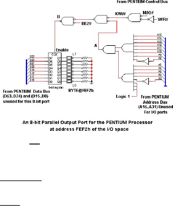
The
logic diagram shown below
shows an 8-bit parallel
output port at address FEF2h
of
the
Pentium's I/O address space. Since
the Pentium allows the
use of some part of
its
data bus
during a transfer, we can use
the BE2# signal in the
address decoder to enable
the
8-bit register. The
following instructions will access
this output port.
mov
dx, 0FEF2h
mov
al, 12h
out
dx, al
The
Pentium does
allow
the use of some part of
its 32-bit accumulator
register EAX. In
case
only 8-bits are to be
transferred, register AL can be used, as
shown in the program
fragment
above. The data byte
12h will be sent to the 8-bit
register over lines
D23..D16.
Since 12h
corresponds to 0001 0010 in binary, this will
cause the LEDs L4 and L1 to
turn
on.
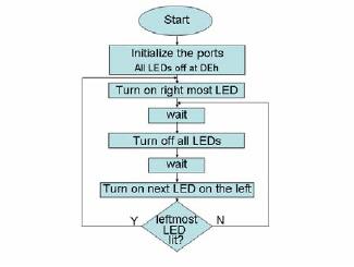
Example
# 3
Problem
statement:
Write an
assembly language program to
turn on the 16 LEDs one by one on
the output
port of
Example #1(lec24). Each LED
should stay on for a
noticeable duration of
time.
Repeat
from the first LED
after the last LED is
turned on.
Solution:
Page
251
Last
Modified: 01-Nov-06

Advanced Computer
Architecture-CS501
________________________________________________________
The
solution is shown in the
text box with a filename:
Example_3.asmfa. The working
of
this
program is explained
below:
The
first two instructions turn
all the LEDs off by
sending a 0 to each bit of
the output
port at
address 222.
mov
r1,0
out
r1,222
Then a 1
is sent to L0 causing it to turn on, and
the program enters a loop
which executes
15 times
to cause the other
LEDs
(L1
through L15) to turn on, one
by ; filename:
Example_3.asmfa
one in
sequence. Register r5 is ;
being
used as loop counter. The
;ALL LEDS ARE turned Off
initially
instructions
;
following
three
movi
r1,0
introduce
a
delay
between
out
r1,222
successive
bit patterns sent to
the
output
port, so that each LED stays
;
;First
LED will be turned on each
time
on for a
noticeable duration of
time.
;
delay1:movi
r2,0
start:
movi r1,1
again1:subi
r2,r2,1
out
r1,222
jnz
r2,[again1]
Starting
with a value of 0 in r2 14, ;
movi
r5,15
this
value is decremented to FFFFh
when
the again1 loop is entered.
;
The
jnz
instruction
will cause r2 to ;DELAY
LOOP
decrement
again and again; thereby ;
executing
the loop 65,535 times. An
delay1: movi
r2,0
estimate of
the delay interval is
again1: subi
r2,r2,1
jnz
r2, [again1]
presented
at the end of this
section.
After
this delay, all the
LEDs are ;
movi
r3,0
; TURN
OFF ALL LEDS
turned
off, and a second delay
loop
out
r3,222
executes.
Finally, the next LED
on
the
left, in sequence, is turned on by
;
delay2:
movi r2,0
the
following two
instructions:
again2:
subi r2,r2,1
shiftl
r1,r1,1
jnz
r2, [again2]
out
r1, 222
After
the left most LED is
turned ;
shiftl
r1,r1,1 ; next LED
ON
on,
the process starts all over
again
out
r1,222
because
of the last jump
subi
r5,r5,1
instruction.
The outermost loop
jnz
r5, [delay1]
executes
indefinitely.
jump
[start]
halt
Estimating
the
Delay
Interval
14
this is
necessary because the immediate
operand with the movi
instruction of
the FALCON-A has a
range of
0h to FFh. This will not give us
the large loop counter
that we need here. So we use
the above
software
trick. An alternate way
would be to use nested
loops, but that will tie up
additional CPU
registers.
Page
252
Last
Modified: 01-Nov-06
Advanced Computer
Architecture-CS501
________________________________________________________
To make
things simple, assume that
the FALCON-A is operating at a
clock frequency of
1 MHz.
Also, assume that the
subi
and
the jnz
instructions
take 3 and 4 clock periods,
respectively,
to execute. Since these two
instructions execute 65,535
times each, we can
use
the following formula to
compute the execution time
of this loop:
ET = CPI
x IC x T = CPI x IC / f
where
CPI
= clocks per instruction
IC
=
instruction count
T
= time
period of the clock,
and
f
=
frequency of the
clock.
Using
the assumed values, we
get
ET =
(3+4) x 65535 / (1x10⁶ ) = 0.
459
sec
Since the
movi
r2, 0 instruction
executes
only
once, the time it takes to
execute is
negligible
and has been ignored in
this
calculation.
Page
253
Last
Modified: 01-Nov-06
Table of Contents:
- Computer Architecture, Organization and Design
- Foundations of Computer Architecture, RISC and CISC
- Measures of Performance SRC Features and Instruction Formats
- ISA, Instruction Formats, Coding and Hand Assembly
- Reverse Assembly, SRC in the form of RTL
- RTL to Describe the SRC, Register Transfer using Digital Logic Circuits
- Thinking Process for ISA Design
- Introduction to the ISA of the FALCON-A and Examples
- Behavioral Register Transfer Language for FALCON-A, The EAGLE
- The FALCON-E, Instruction Set Architecture Comparison
- CISC microprocessor:The Motorola MC68000, RISC Architecture:The SPARC
- Design Process, Uni-Bus implementation for the SRC, Structural RTL for the SRC instructions
- Structural RTL Description of the SRC and FALCON-A
- External FALCON-A CPU Interface
- Logic Design for the Uni-bus SRC, Control Signals Generation in SRC
- Control Unit, 2-Bus Implementation of the SRC Data Path
- 3-bus implementation for the SRC, Machine Exceptions, Reset
- SRC Exception Processing Mechanism, Pipelining, Pipeline Design
- Adapting SRC instructions for Pipelined, Control Signals
- SRC, RTL, Data Dependence Distance, Forwarding, Compiler Solution to Hazards
- Data Forwarding Hardware, Superscalar, VLIW Architecture
- Microprogramming, General Microcoded Controller, Horizontal and Vertical Schemes
- I/O Subsystems, Components, Memory Mapped vs Isolated, Serial and Parallel Transfers
- Designing Parallel Input Output Ports, SAD, NUXI, Address Decoder , Delay Interval
- Designing a Parallel Input Port, Memory Mapped Input Output Ports, wrap around, Data Bus Multiplexing
- Programmed Input Output for FALCON-A and SRC
- Programmed Input Output Driver for SRC, Input Output
- Comparison of Interrupt driven Input Output and Polling
- Preparing source files for FALSIM, FALCON-A assembly language techniques
- Nested Interrupts, Interrupt Mask, DMA
- Direct Memory Access - DMA
- Semiconductor Memory vs Hard Disk, Mechanical Delays and Flash Memory
- Hard Drive Technologies
- Arithmetic Logic Shift Unit - ALSU, Radix Conversion, Fixed Point Numbers
- Overflow, Implementations of the adder, Unsigned and Signed Multiplication
- NxN Crossbar Design for Barrel Rotator, IEEE Floating-Point, Addition, Subtraction, Multiplication, Division
- CPU to Memory Interface, Static RAM, One two Dimensional Memory Cells, Matrix and Tree Decoders
- Memory Modules, Read Only Memory, ROM, Cache
- Cache Organization and Functions, Cache Controller Logic, Cache Strategies
- Virtual Memory Organization
- DRAM, Pipelining, Pre-charging and Parallelism, Hit Rate and Miss Rate, Access Time, Cache
- Performance of I/O Subsystems, Server Utilization, Asynchronous I/O and operating system
- Difference between distributed computing and computer networks
- Physical Media, Shared Medium, Switched Medium, Network Topologies, Seven-layer OSI Model