 |
THE LOGIC BLOCK: Analogue to Digital Conversion, Logic Element, Look-Up Table |
| << LAST IN-FIRST OUT (LIFO) MEMORY |
| SUCCESSIVE –APPROXIMATION ANALOGUE TO DIGITAL CONVERTER >> |
CS302 -
Digital Logic & Design
Lesson
No. 44
THE
LOGIC BLOCK
Each
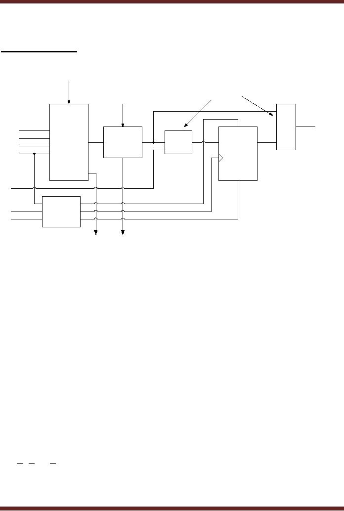
Logic Block consists of a
several Logic elements. The
details of the Logic
Element
are shown in figure
44.1.
Programmable
Carry
In
To
Select
Interconnect
Data
from
Cascade
programmable
In
interconnects
Look
Cascade
Up
Logic
Table
Flip-Flop
Clock/Clear/
Preset
Select
Logic
Carry
Cascade
Out
Out
Figure
44.1
Block
diagram of a Logic
Element
The
Logic Element
The
Look-Up Table LUT has
4-inputs and can be
programmed as a logic
function
generator.
The LUT can be programmed to
produce SOP functions or
logic functions such
as
adders
and comparators. When the
LUT is configured as an adder
the Carry In and Carry
Out
inputs
and outputs allow for
adder expansion by connecting
more adders. The Cascade
Logic
allows
one LUT to be cascaded with
another LUT in other logic
units. There are
two
Programmable
selects, the first
Programmable selects allows
selection of either
the
combinational
functions from the LUT
output or a direct input to be
connected to the input of
a
flip-flop.
The second Programmable
select allows selection of
the combinational function
from
the
LUT output or the registered
functions from the flip-flop
output. The
clock/Clear/Preset
Select
Logic controls the operation
of the flip-flop through the
Clear and Select
Asynchronous
signals
and the Clock Synchronous
signal.
The
Look-Up Table
The
Look-Up Table shown in the
Logic Element is implemented
using a memory
element
that can be programmed to
implement different logic
functions. Two examples of
LUT
programmed to
generate a logic function
and to implement a full-adder
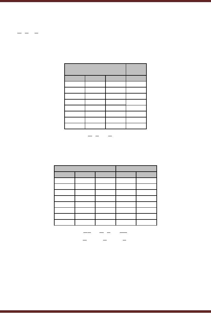
are shown. Table
44.1
In the
first example illustrated by
Table 44.1a a three variable
SOP function
F = ABC + ABC + ABC
is implemented.
A memory having 8 locations
and storing a single
bit
value at
each location is required to
implement the three variable
function. The three
bit
address
lines which are used to
select one out of eight
memory locations represents
the three
function
variables A, B and C respectively.
The product terms that
are included in the
function
439
CS302 -
Digital Logic & Design
are
represented by memory locations
that store logic 1 binary
value. The product terms or
the
Min-terms
that are missing from
the function are represented
by memory locations that
store
logic 0
value. In the function
shown, memory locations 2, 5
and 7 which represent the
product
terms
ABC, ABC and ABC
respectively
have logic 1 values stored.
Thus when ever
addresses 2, 5
or 7 are issued, the data
output is a 1 for all other
addresses the data output
is
a 0.
Address
Input
Data
Output
A
B
C
F
0
0
0
0
0
0
1
0
0
1
0
1
0
1
1
0
1
0
0
0
1
0
1
1
1
1
0
0
1
1
1
1
F = ABC + ABC + ABC
Table
44.1a
LUT
programmed to generate a
function
Address
Input
Data
Output
A
B
Cin
Sum
Cout
0
0
0
0
0
0
0
1
1
0
0
1
0
1
0
0
1
1
0
1
1
0
0
1
0
1
0
1
0
1
1
1
0
0
1
1
1
1
1
1
Sum
=
ABC
+
ABC
+
ABC
+
ABC
C out = ABC + ABC + ABC + ABC
Table
44.1b
LUT
Programmed as Full-Adder
A Single
bit Full-Adder can be
similarly implemented by using a
memory which has
three
storage locations, each
location storing two bits. A
single bit full-adder has
three input
variables A, B
and Cin
and
two output variables Sum
and Cout.
The three address lines
which
select
one out of eight memory
locations are connected to
the three input variables A,
B and
Cin. The eight two
bit memory locations are
programmed to represent the
Sum and Cout
functions. An
address 110 represents the
variables A=1 and B=1
and Cin
= 0. The
Sum output
440

CS302 -
Digital Logic & Design
should be 0
and the Cout should be 1 which is
represented by the data
output 01 corresponding
to the
address 110.
Analogue to
Digital Conversion
Digital
systems process digital
information. The input and
the output to the
digital
systems is in
digital binary format. Real
world quantities are in
analogue form, which
are
converted
into digital format for
processing by the digital
system. The processed
digital output
has to be
converted back into analogue
format. Mobile phones
convert the analogue
speech
signal
into a digital signal which
is processed digitally. The
digital signal which is
received is
converted
back to an analogue form
which one hears. Digital
thermometers measure
temperature
which is in analogue form.
The analogue signal is
converted into digital
format
which is
displayed in the form of
numbers representing the
temperature value.
Measuring
instruments
such as digital voltmeters
also sample an electrical
signal in its analogue
form.
The
analogue samples are
digitized and displayed in
the form of numbers
representing voltage
values.
CDs which store digital
audio and video files
have the original audio
and video
analogue
signals converted into
digital format for storage
on CDs. To replay the audio
or video
file
the digital information is
converted back into analogue
form. Industrial controller
system
sample
analogue values, digitize
the sampled values, process
the digitized data and
convert
the
digitized processed information
into corresponding analogue
outputs.
Analogue
signals are converted into
Digital signals by Analogue to
Digital (A/D)
converters.
The conversion of the
analogue signal into a
corresponding digital signals is
done
by first
sampling the analogue signal
and holding it stable for
the A/D converter to convert
the
signal
into a digital value.
Sample
and Hold
Operation
A sample
and hold circuit performs
two important operations.
The analogue signal
is
sampled at
regular sampling intervals to
take sufficient number of
discreet values at points
on
the
analogue waveform. The more
samples are taken the
more accurate is the
representation
of the
original analogue signal.
The sampling frequency
according to the Nyquist
Criteria
should be
twice the maximum frequency
of the highest analogue
frequency. A sampled
value
has to be
held stable for a certain
minimum time to allow the
A/D converter to convert
the
sample
values into equivalent
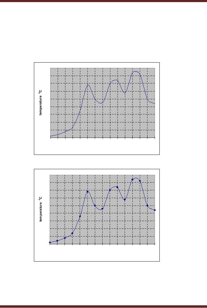
digital values. Figure 44.2a
shows an input analogue
signal
representing
temperature varying with
time. To convert the
analogue signal it is sampled
at
regular
intervals. The analogue
signal which is sampled at 15
equal intervals is shown in
figure
44.2b.
The number of samples
determine the accuracy of
the digitized signal. If the
15
samples
are plotted the resulting
signal represents reconstructed
analogue signal based
on
the 15
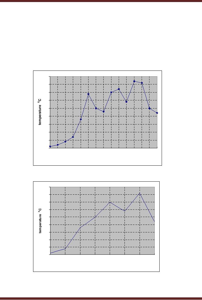
samples. Figure 44.2c. The
reconstructed signal is not an
exact replica of the
original
analogue
signal but is similar. The
exactness of the reconstructed
signal depends upon
the
number of
samples. If the number of
samples are few then
the reconstructed signal
losses its
resemblance to
the original signal. Figure
44.2d. The signal with
fewer samples then
the
desired
number of samples that are
required to accurately reconstruct
the signal is known
as
an under
sampled signal. The under
sampled signal is shown to
lose the information in
the
original
signal when it is reconstructed. If
the original signal is over
sampled by increasing
the
number of
samples beyond 15, the
reconstructed signal will be a
very accurate
representation
of the
original signal however
processing too many samples
may require too much
processing
time.
441
CS302 -
Digital Logic & Design
45
40
35
30
25
20
15
10
5
0
1
2
3
4
5
6
7
8
9
10
11
12
13
14
15
time
Figure
44.2a
Continuous
signal showing temperature
varying with time
45
42
41
40
37
35
35
34
30
29
25
25
25
23
22
20
18
15
10
7
5
4
2
1
0
1
2
3
4
5
6
7
8
9
10
11
12
13
14
15
time
Figure
44.2b Sampling the
Continuous Signal at 15 equal
intervals
442
CS302 -
Digital Logic & Design
45
42
41
40
37
35
35
34
30
29
25
25
25
23
22
20
18
15
10
7
5
4
2
1
0
1
2
3
4
5
6
7
8
9
10
11
12
13
14
15
samples
Figure
44.2c Reconstructed Signal by
plotting 15 sampled
values
45
40
35
30
25
20
15
10
5
0
1
3
5
7
9
11
13
15
samples
Figure
44.2d Reconstructed Signal by
plotting 7 sampled
values
443
CS302 -
Digital Logic & Design
The
number of samples that are
essential to accurately represent
the original signal
is
determined by
the Nyquist Criteria which
requires that the sampling
frequency should be
twice
the
frequency of the sampled
signal. Assuming the
original signal to have a
frequency of 50
Hz,
the sampling which allows
accurate reconstruction of the
signal should be carried out
at
100
Hz.
The
sampled signal at Nyquist
frequency have to be held
stable for a minimum
time
period to
allow the A/D converter to
convert the analogue sample
into a digital value. If
the
sampled
signal is not held stable,
the A/D converted would
not have enough time to
accurately
convert
the signal into a digital
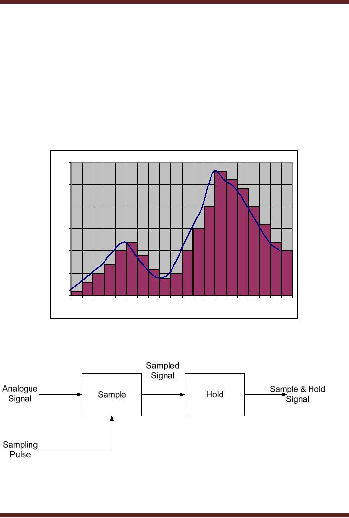
value. The samples that
are held stable for
converting into
digital
values by the sample and
hold circuit are depicted by
a staircase signal shown in
figure
44.3.
30
28
26
24
25
20
20
20
16
15
15
12
12
10
10
10
9
10
7
6
5
5
4
5
3
1
0
1
2
3
4
5
6
7
8
9 10 11 12 13 14 15 16 17 18
19 20
Figure
44.3a Sample and Hold
signal
Figure
44.3b Sample and Hold
Circuit
Quantization
444
CS302 -
Digital Logic & Design
The
process of converting the
analogue signal into a
digital representation (code)
is
known as
quantization. The number of
bits that are used to
represent the digital
code
determine
the accuracy of the
digitized signal. An analogue
220 volt signal can be
represented
in digital
terms by a 2-bit binary
number. The four possible
digital values 00, 01, 10
and 11
represent
four levels of the input
220 volt analogue signal.
The binary value 00
represents 0
volts, 01
represents 73 volts, 10 represents
146 volts and 11 represents
220 volts. Since
four
values
can be represented, therefore
analogue voltages in the
ranges 37 to 109 are
represented by
binary 01. Similarly voltage
ranges between 110 to 183
are represented by
binary
10. If a three bit
representation is used then
the range of analogue
signals represented
by the
eight, 3-bit values is
reduced thereby increasing
the accuracy.
30
30
28
30
30
28
23
21
23
21
16 15
15
16
15
15
11
10
9
11
8
10
9
8
0
0
1
2
3
4
5
6
7
8
9
10
11
12
13
1
2
3
4
5
6
7
8
9
10
11 12 13
Figure
44.4a Analogue Signal
Figure
44.4b
Sample &
Hold Signal
3
3
3
3
2
2
2
2
1
1
1
1
0
1
2
3
4
5
6
7
8
9
10
11 12 13
Figure
44.4c Digitized
Signal
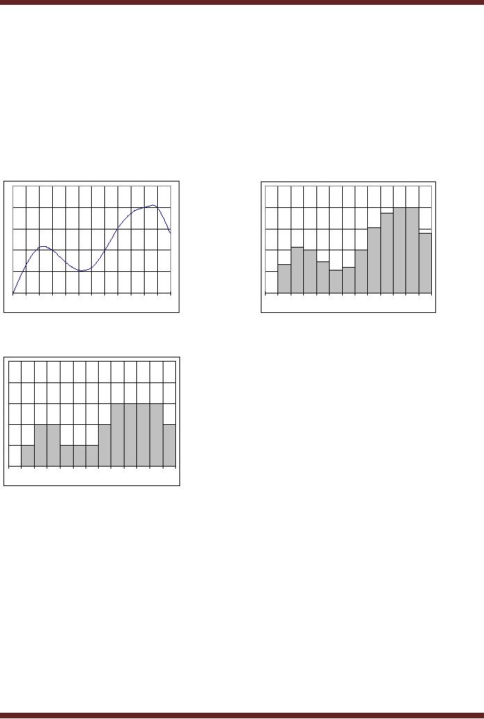
In figure
44.4 the representation of an
analogue signal using 2 bits
or four quantization
levels is
shown. The original signal
has analogue value range
from 0 to a peak value of
31.
Figure
44.4a. The analogue signal
is sampled, the output of
the Sample and Hold
circuit is
shown in
figure 44.4b. The sampled
values range between 0 and
30. The sampled signal
is
digitized
using four quantization
levels or 2-bits. Figure
44.4c. The original signal
having
values in
the range 0 to 7.5 are
represented by a digital representation
00. Analogue values
in
the
range 8 to 14.5 are
represented by a digital representation
01. Analogue values in
the
range 15 to
22.5 are represented by
digital representation 10 and
the values ranging
between
23 and 30
are represented by digits
11. If the quantization
level is quadrupled to 16 levels
the
digitized
representation of the analogue
signal becomes more
accurate. Figure
44.5.
445
CS302 -
Digital Logic & Design
30
30
30
30
28
28
23
23
21
21
16
15
15
16
15
15
11
10
11
9
10
8
9
8
0
0
1
2
3
4
5
6
7
8
9
10
11
12
13
1
2
3
4
5
6
7
8
9
10
11 12 13
Figure
44.5a Analogue Signal
Figure
44.5b
Sample &
Hold Signal
15
15
14
12
11
8
8
8
6
5
5
4
0
1
2
3
4
5
6
7
8
9
10
11 12 13
Figure
44.5c Digitized
Signal
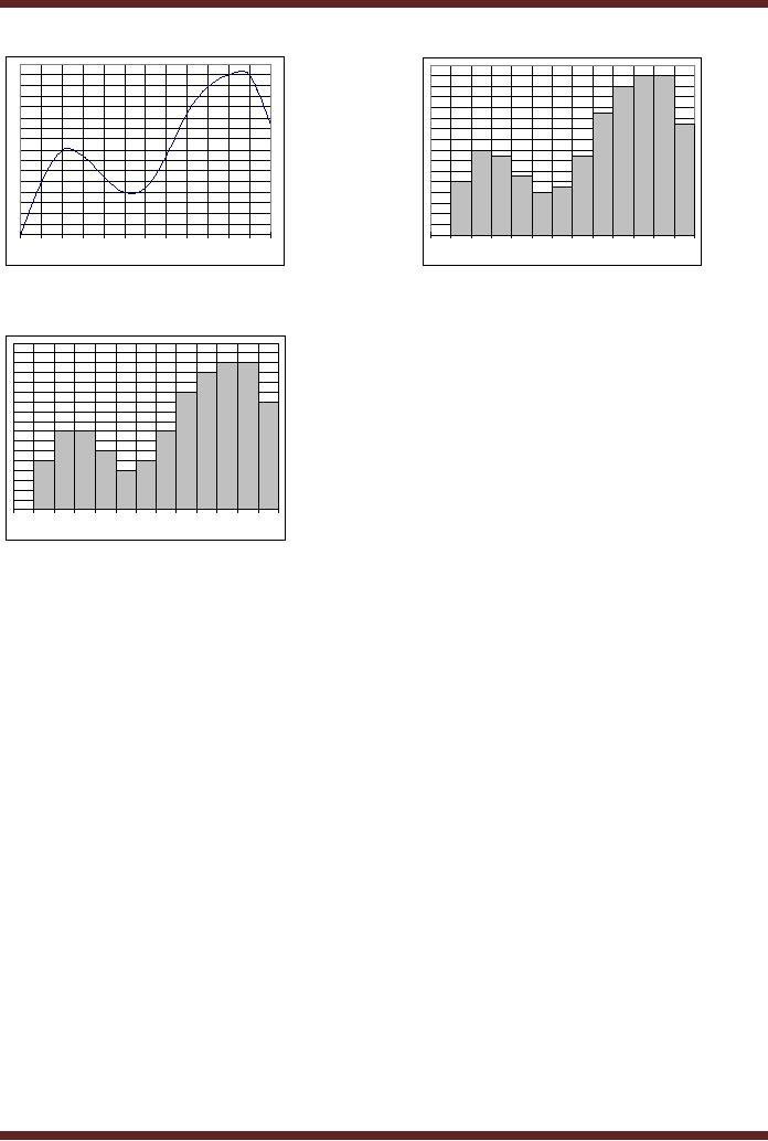
In figure
44.5, the analogue signal is
shown to be digitized using a 16
level
quantization.
The digitized signal shown
in figure 44.5c closely
resembles the analogue
signal
as compared to
the 4 level quantized signal
shown in figure
44.4c.
Operational
Amplifier (Op-Amp)
Operational
Amplifier is a linear amplifier
which has two inputs
(inverting and non-
inverting)
and one output. It has a
high voltage gain, high
input impedance and low
output
impedance.
The Op-Amp amplifies the
difference signal between
its inverted and
non-inverted
inputs.
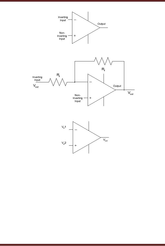
Figure 44.6a
The
Op-Amp is used as an inverting
amplifier and as a comparator.
When the Op-Amp
is used as an
inverting amplifier, the
input signal is applied at
its Inverted input through
a
series
resistance Ri.
The output of the Op-Amp is
connected to the inverted
input through a
feedback
resistance Rf.
Figure 44.6b. The voltage
gain of the Inverting
Amplifier is given by
the
relation
Vout/Vin = -
Rf/Ri
When
the Op-Amp is used as a
comparator two voltages are
applied at the
inputs,
when
these voltages differ by a
very small amount the
output of the Op-Amp is
driven into one
of its
two saturated output sates
logic high or low depending
upon which of the two
input
voltages is
higher. Figure 44.6c
446
CS302 -
Digital Logic & Design
Figure
44.6a Op-Amp
Figure
44.6b Op-Amp as an Inverting
Amplifier
Figure
44.6c Op-Amp as a
Comparator
Analogue to
Digital converters use
Op-Amps as an Integrator and
Comparator. An
Integrator
integrates the input
voltage. An Integrator is implemented by
replacing the
feedback
resistance
Rf by a
Capacitor.
Flash
Analogue-to Digital
Converter
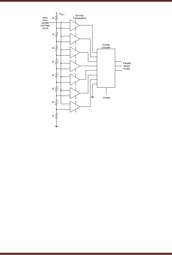
The
Flash A/D converter is based
on a resistor potential divider,
where multiple
resistors of
identical value form a
voltage divider. A reference
voltage is applied at one
end of
the
potential divider which
divides the voltage equally
across all the resistors.
The input
analogue
voltage is applied at the
non-inverting inputs of a set of
Op-Amp based
comparators.
The
inverting input of each
comparator is connected to the
resistive voltage divider
which
provides
reference voltages for all
the comparators. If the
input voltage is larger than
the
reference
voltage the output of the
comparator is logic high
otherwise it is logic low.
The
outputs of
all the comparators are
connected to the input of a
priority encoder which
converts
the
comparator outputs to a binary
coded equivalent value.
Figure 44.7a.
447
CS302 -
Digital Logic & Design
Figure
44.7a Flash A/D
Converter
The
analogue input sampled
signal is applied at the
input of the seven
comparators.
The
inverted input of each of
the seven comparators is
connected to voltage divider
circuit
made up of
eight resistors having the
same value R. A reference
voltage +VREF is connected at
the
top end of the voltage
divider circuit and the
lower end of the voltage
divider is connected
to the
ground. The voltage drops
across the eight resistors
starting from the top
most resistor
are
VREF, 7/8VREF, 6/8VREF, 5/8VREF, 4/8VREF, 3/8VREF, 2/8VREF and
1/8VREF respectively. If the
input
sampled voltage input is
greater than the reference
input voltage for any
comparator, the
comparator
output is logic 1, otherwise
the output is logic 0. The
inputs of an eight-to-three
Priority
Encoder are connected to the
comparator outputs. The
lowest priority input of
the
Encoder is
grounded. The priority
encoder is enabled at each
sampled input and a 3-bit
code
representing
the value of the input
sample appears at the
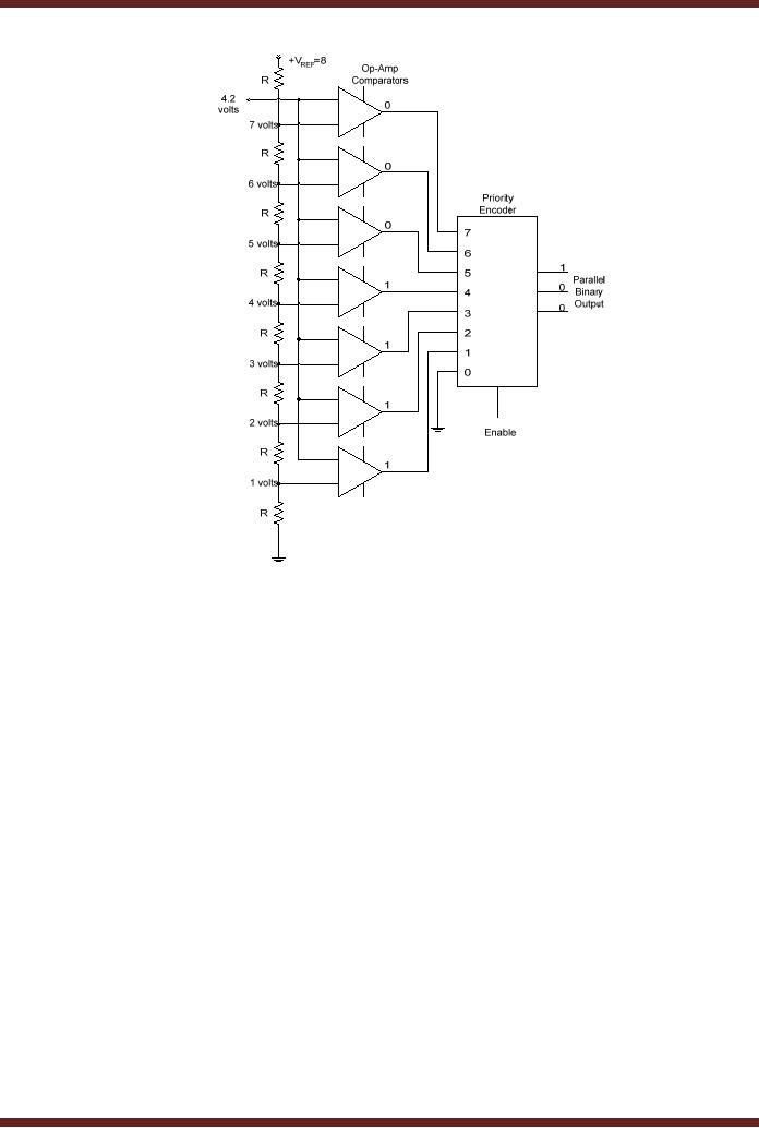
output. Consider an example,
the
input
sample is 4.2 volts. The
reference voltage VREF is equal to 8 volts, the
seven reference
voltages
applied at the inverted
inputs of the seven
comparators starting from
the first
comparator
are 7, 6, 5, 4, 3, 2 and 1 volts
respectively. With an input of
4.2 volts the outputs
of
the
first three comparators are
set to logic 0 and the
outputs of the lower four
comparators are
set to
logic 1 which sets the
encoders first three inputs
to inactive-low and the next
four inputs
to active
high. The highest priority
input the encoder outputs
100 which is binary
equivalent of
4. Figure
44.7b.
448
CS302 -
Digital Logic & Design
Figure
44.7b 3-bit FLASH A/D
Converter
The
3-bit Flash converter
requires seven comparators, a
4-bit Flash converter
requires
fifteen
converters. A large number of
comparators are required to
implement a reasonable-
sized
converter. The advantage is
that the conversion is done
in parallel and the
binary
equivalent
value is available at the
output of the converter
almost instantaneously.
Flash
converters
are used for high
speed conversion applications
such as conversion of
analogue
video
signals into digital
signals. For accurate
reproduction of the digital
signal, Flash A/D
converters
are based on high number of
Quantization levels which
requires the use of
many
Op-Amp
based Comparators which
makes the Flash converters
expensive and power
hungry
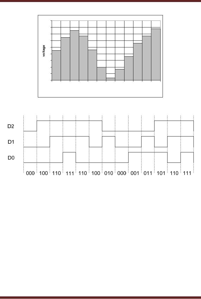
Figure
44.8 shows a set of sampled
analogue voltage inputs
applied at the input of
the
Flash
converter shown in the
figure 44.7. The reference
voltage of the Flash
converter is set to
8 volts. At
each sampling interval an
enable pulse allows the
Flash converter to convert
the
corresponding
analogue input voltage
sample to be converted and
represented in its
binary
form.
Figure 44.9.
449
CS302 -
Digital Logic & Design
9
7.8
7.5
8
6.7
6.7
6.5
7
5.6
6
4.6
4.5
5
3.6
4
3
2
1.7
2
1
0.4
0
1
2
3
4
5
6
7
8
9
10
11
12
time
Figure
44.8
Input
analogue voltage
samples
Figure
44.9
Binary
output representing input
analogue voltage
samples
Dual-Slope
Analogue to Digital
Converter
The
Dual-Slope A/D converter is
used in digital voltmeters
and other types of
measuring
instruments. A Dual-Slope A/D
converter is slower than the
Flash Converter. The
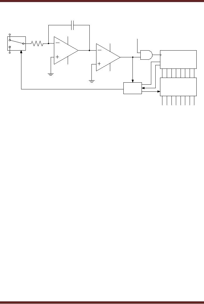
circuit
diagram of the converter is
shown. Figure 44.10. The
converter consists of a
switch.
Initially,
the switch connects the
circuit to the input
analogue voltage which is to be
converted
into
its corresponding binary
representation. During the
conversion process the
switch
connects
the circuit to a negative
reference voltage. The
switching between the input
voltage
and
the reference voltage allows
a capacitor connected between
the Op-Amp output and
input
to be charged
and discharged. An Op-Amp
based Integrator integrates
the analogue input
voltage
over a fixed period of time.
An Op-Amp based Comparator
compares the output of
the
Integrator
with the ground voltage to
enable or disable a counter
circuit. A counter and
latch
counts
the binary output
corresponding to the analogue
input value. A logic control
circuit is
used to
switch between analogue
voltage input and the
reference voltage. It
also
enables/disables
the latch.
450
CS302 -
Digital Logic & Design
C
Analogue
Input
(Vin)
CLK
R
Switch
A1
A2
-VREF
Counter
R
n
Integrator
CLEAR
(ramp
generator)
Comparator
Control
Latches
Logic
En
Switch
Control
D0
D7
Binary or
BCD
Output
Figure
44.10 Dual-Slope A/D
Converter
The
first Op-Amp is connected as an
Integrator. Initially, the
counter is reset and has
a
zero
count. The Input switch is
connected to the Analogue
input which is to be converted
into
equivalent
binary value. The counter is
reset to count zero by the
Control Logic circuit. It
also
sets
the switch to the Analogue
input voltage. The Input
analogue voltage is assumed to
be
constant
for the duration of the
conversion process. Due to
the high input impedance of
the
Integrator,
the current from the
Analogue Input source flows
through the Resistor R and
the
Capacitor C.
The Capacitor will charge
and there will be a
negative-going linear voltage
ramp
at the
output of A1.
The non-inverted input of
the Comparator is connected to
the ground,
therefore as
the inverted input of the
comparator becomes negative,
the output changes to
logic 1.
The Logic 1 output triggers
the Control Logic which in
turn resets the counter.
The
logic 1
output enables the AND gate
which allows the clock
signal to be applied at the
counter
clock
input which increments the
counter at each clock pulse.
The Integrator output
remains at
negative
voltage as the negative-going
linear ramp continues the
integration process. As
the
counter
count reaches its maximum
count value (terminal
count), it rolls over and
sends a
signal to
the control Logic circuit
which switches the switch to
VREF.
The
Capacitor which is
charged to a
positive input voltage
discharges resulting in a positive
going slope at the
output
of integrator.
When the voltage at the
inverted input of the
comparator reaches zero
volt, the
comparator
output become logic 0
disabling the AND gate and
therefore inhibiting the
counter
from
counting. The Control Logic
circuit sends a pulse which
loads the latch with
the count
value.
Table
44.2 depicts the working of
the Dual-Slope A/D
converter. At interval t = 0
the
converter is
switched to the Vin input which is assumed to
remain constant during
the
conversion
operation. The capacitor
starts charging at a constant
rate. The output of
the
Integrator
(voltage output) decreases at
constant slope (-V). The
output of the comparator
is
set to 1
enabling the clock signal
and incrementing the
counter. The converter
remains
connected to
Vin for a fixed
duration determined by time
interval t = n. The duration of
the
interval is
determined by the maximum
count value of the counter.
During this interval
the
capacitor
has charged to a maximum
value determined by the
input voltage. At time
interval t =
n, the
counter reaches its terminal
count and rolls over.
The logic control circuit
switches to
451
CS302 -
Digital Logic & Design
Vref. At interval
t=n+1 the capacitor begins
to discharge as now it is connected to a
negative
voltage
-Vref . The Integrator
output starts increasing
towards a 0 voltage at a constant
rate.
The
output of the Comparator is
logic high allowing the
counter to count. At interval t =
n+m
the
capacitor has completely
discharged and the
comparator inputs become
equal setting its
output to 0.
The clock signal is
disabled, disabling the
counter from counting. The
count value
represents
the input voltage. Interval
m is determined by the magnitude of
the charge stored
on the
capacitor. Higher the
voltage stored on the
capacitor longer it will
take to discharge to 0
volts,
thereby allowing the counter
to a larger count value. If
the input analogue voltage
is
small,
the capacitor will be
charged to a smaller voltage. It
will therefore discharge in a
shorter
interval of
time allowing the counter to
count to a small
value.
Time
Input
Output
of
Output
of
Clock
Counter
interval
t
signal
Integrator
Comparator
Input
0
Vin
-V
1
enabled
Counting
1
Vin
-V
1
enabled
Counting
n
Vin
-V
1
enabled
Terminal
count reached.
Counter
reset.
Switched to
Vref
n+1
-Vref
-V
1
enabled
Counting
n+2
-Vref
-V
1
enabled
Counting
n+m
-Vref
0
0
disabled
Binary
value representing
Vanalogue
Table
44.2
Operation of
Dual-Slope A/D
Converter
452
Table of Contents:
- AN OVERVIEW & NUMBER SYSTEMS
- Binary to Decimal to Binary conversion, Binary Arithmetic, 1’s & 2’s complement
- Range of Numbers and Overflow, Floating-Point, Hexadecimal Numbers
- Octal Numbers, Octal to Binary Decimal to Octal Conversion
- LOGIC GATES: AND Gate, OR Gate, NOT Gate, NAND Gate
- AND OR NAND XOR XNOR Gate Implementation and Applications
- DC Supply Voltage, TTL Logic Levels, Noise Margin, Power Dissipation
- Boolean Addition, Multiplication, Commutative Law, Associative Law, Distributive Law, Demorgan’s Theorems
- Simplification of Boolean Expression, Standard POS form, Minterms and Maxterms
- KARNAUGH MAP, Mapping a non-standard SOP Expression
- Converting between POS and SOP using the K-map
- COMPARATOR: Quine-McCluskey Simplification Method
- ODD-PRIME NUMBER DETECTOR, Combinational Circuit Implementation
- IMPLEMENTATION OF AN ODD-PARITY GENERATOR CIRCUIT
- BCD ADDER: 2-digit BCD Adder, A 4-bit Adder Subtracter Unit
- 16-BIT ALU, MSI 4-bit Comparator, Decoders
- BCD to 7-Segment Decoder, Decimal-to-BCD Encoder
- 2-INPUT 4-BIT MULTIPLEXER, 8, 16-Input Multiplexer, Logic Function Generator
- Applications of Demultiplexer, PROM, PLA, PAL, GAL
- OLMC Combinational Mode, Tri-State Buffers, The GAL16V8, Introduction to ABEL
- OLMC for GAL16V8, Tri-state Buffer and OLMC output pin
- Implementation of Quad MUX, Latches and Flip-Flops
- APPLICATION OF S-R LATCH, Edge-Triggered D Flip-Flop, J-K Flip-flop
- Data Storage using D-flip-flop, Synchronizing Asynchronous inputs using D flip-flop
- Dual Positive-Edge triggered D flip-flop, J-K flip-flop, Master-Slave Flip-Flops
- THE 555 TIMER: Race Conditions, Asynchronous, Ripple Counters
- Down Counter with truncated sequence, 4-bit Synchronous Decade Counter
- Mod-n Synchronous Counter, Cascading Counters, Up-Down Counter
- Integrated Circuit Up Down Decade Counter Design and Applications
- DIGITAL CLOCK: Clocked Synchronous State Machines
- NEXT-STATE TABLE: Flip-flop Transition Table, Karnaugh Maps
- D FLIP-FLOP BASED IMPLEMENTATION
- Moore Machine State Diagram, Mealy Machine State Diagram, Karnaugh Maps
- SHIFT REGISTERS: Serial In/Shift Left,Right/Serial Out Operation
- APPLICATIONS OF SHIFT REGISTERS: Serial-to-Parallel Converter
- Elevator Control System: Elevator State Diagram, State Table, Input and Output Signals, Input Latches
- Traffic Signal Control System: Switching of Traffic Lights, Inputs and Outputs, State Machine
- Traffic Signal Control System: EQUATION DEFINITION
- Memory Organization, Capacity, Density, Signals and Basic Operations, Read, Write, Address, data Signals
- Memory Read, Write Cycle, Synchronous Burst SRAM, Dynamic RAM
- Burst, Distributed Refresh, Types of DRAMs, ROM Read-Only Memory, Mask ROM
- First In-First Out (FIFO) Memory
- LAST IN-FIRST OUT (LIFO) MEMORY
- THE LOGIC BLOCK: Analogue to Digital Conversion, Logic Element, Look-Up Table
- SUCCESSIVE –APPROXIMATION ANALOGUE TO DIGITAL CONVERTER