 |
CS302 -
Digital Logic & Design
Lesson
No. 39
MEMORY
Sequential
circuits can not operate
without a memory element.
Memory elements used
in Sequential
circuits are relatively
small and store few
binary bits of information.
Large
memories
capable of storing very
large amounts of information
are used in Computer
systems.
A computer
which executes an application
program has the application
stored in the form of
program
instructions in large
memories.
Memories
store data in units that
have one, four, eight or
higher number of
bits.
Smallest
unit of binary data is a
bit. Data is also handled in
a 4-bit unit called a
Nibble. In many
applications
the data is handled as an
8-bit unit called a byte,
which is a combination of two
4-
bit
units that are called
Nibbles. A complete unit of
information is sometimes called a
Word and
consists of
one or more bytes.
Each
storage element of a memory
can either store a logic 0
or a logic 1 and is called
a
cell.
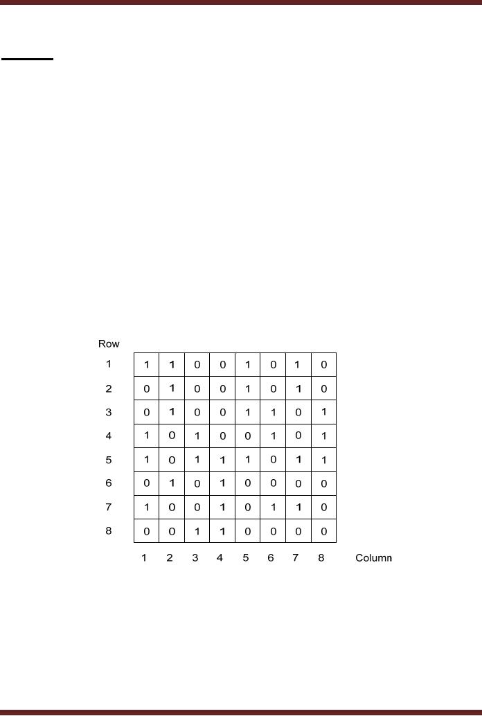
Memories are arranged in an
array and each cell
can be identified by specifying a
row
and a
column number. Figure 39.1.
Each square in the diagram
represents a memory
cell
capable of
storing a binary 1 or 0. The
first eight bits of binary
information 11001010 in the
first
row
are stored in eight cells.
The addresses of the eight
consecutive cells staring
from the left
most
cell are (1,1), (1,2),
(1,3), (1,4), (1,5), (1,6),
(1,7) and (1,8) representing
the first row
and
columns 1 to 8
respectively. Individual cells at
row 5 and column 3 have a
binary 1 and a cell
at row 6
and column 7 have a binary 0
stored.
Figure
39.1
64-cell
Memory Array
Memory
Organization
The
Memory array can be
organized in several ways
depending on the unit of
data.
The
64-cell array organized as 8 x 8
cell array is considered as an 8
byte memory, that is,
it
394
CS302 -
Digital Logic & Design
has
eight locations and each
location stores a single
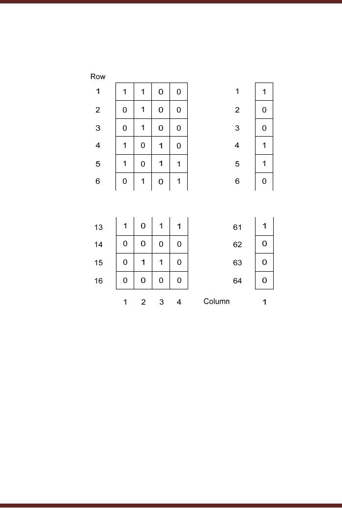
byte. The 64-cell array
organized as 4 x
16 cell
array stores 16 nibbles and
if organized as 1 x 64 stores 64 single
bit values. The 4 x
16 memory
array allows data to be
accessed in the form of
4-bit nibbles. The 1 x 64
array
allows
data to be accessed in units of 1
bit. Figure 39.2.
Figure
39.2
Memory
Organized as 4 x 16 and 1 x 64
Arrays
A memory is
identified by the number of
units it can store times
the unit size, thus
the 8
x 8 memory is
identified as an 8 Byte memory,
the 16 x 4 memory is used as a 16
Nibble
memory
and the 64 x 1 is known as a 64
bit memory. Practical memory
chips are organized
as
16 K x 8 memory,
storing 16K bytes or 16 x
1024 = 16384 bytes. A 32 K x 4
memory stores
32K
nibbles or 32 x 1024 = 32768
nibbles.
Memory
Capacity and
Density
Each
memory array has a maximum
capacity to store information in
the form of bits.
Thus a 16 K x 8
memory, stores 16K bytes or
16 x 1024 = 16384 bytes or
131072 bits. A 32 K
x 4 memory
stores 32K nibbles or 32 x
1024 = 32768 nibbles or
131072 bits. The total
number
of cells in
each case is 131072. Memory
density on the other hand
specifies the number of
bits
stored
per unit area. More
the number of bits stored in
a unit area more dense
the memory,
that
is, more bits are
stored in less space. The
capacity and the density of
a memory are
determined by
the total number of cells
implemented in a unit
area.
395
CS302 -
Digital Logic & Design
Memory
Signals and Basic Operations
on Memory
Two
basic operations are
performed on memories, that
is, reading of information
from
the
memory and writing of data
to the memory. To support
the two read and
write operations
memories
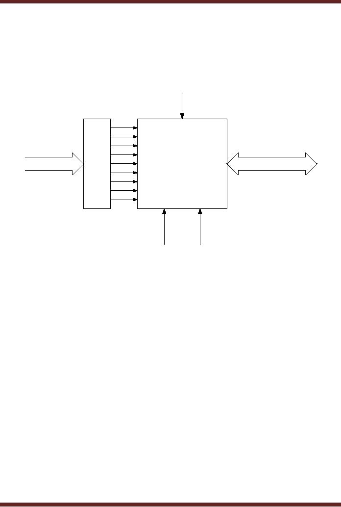
provide several signals.
Figure 39.3.
Memory
Select
Address
Decoder
Memory
Array
Address
Data
Bus
Bus
Read
Write
Figure
39.3
Block
Diagram of a Read-write
Memory
Read
and Write Signals
Read/Write
signals are required to
configure the memory for
read and write
operation.
Memory
chips have a single
Read/Write signal. When the
signal is set to high it
allows data to
be read
from the memory. When
the signal is set to low
data is written into the
memory. Some
memory
chips have two separate
Read and Write signals.
The read and write
signals are
separately
asserted to control the Read
and Write operation.
Address
Signals
Address
signals are required to
specify the location in the
memory from which
information is
accessed (read or written). A
set of parallel address
lines known as the
address
bus
carry the address
information. The number of
bits (lines) comprising the
address bus
depends
upon the size of the
memory. For example, a
memory having four locations
to store
data
has four unique addresses
(00, 01, 10, 11)
specified by a 2-bit address
bus. The size of
the
address bus depends upon
the total addressable
locations specified by the
formula 2n,
where n is
the number of bits. Thus
24=16 (n=4)
specifies 4 bits to uniquely
identify 16 different
locations.
Data
Signals
Data
lines are required to
retrieve the information
from the memory array
during a read
operation
and to provide the data
that is to be stored in the
memory during a write
operation.
As the
memory reads or writes one
data unit at a time
therefore the data lines
should be equal
to the
number of data bits stored
at each addressable location in
the memory. A memory
organized as a
byte memory reads or writes
byte data values, therefore
the number of data
396
CS302 -
Digital Logic & Design
lines or
the size of the data
bus should be 8-bits or 1
byte. A memory organized to
store nibble
data
values requires a 4-bit wide
data bus. Generally, the
wider the data bus
more data can be
accessed at
each read or write
operation.
Memory
Select or Enable
Signal
In a computer
system there are more
than one memory chips to
store program
information. At
any particular instant a
read or write operation is
carried out on a
single
addressable
location. The unique
location can only be
accessed in one of the
several memory
chips,
thus a single memory chip
has to be selected before a
read or write operation can
be
carried
out. All memory chips
have a chip enable or chip
select signal which has to
be
activated
before the memory can be
accessed.
Memory
Read operation
Memory
Read operation is carried
out by first selecting the
memory chip by
activating
the
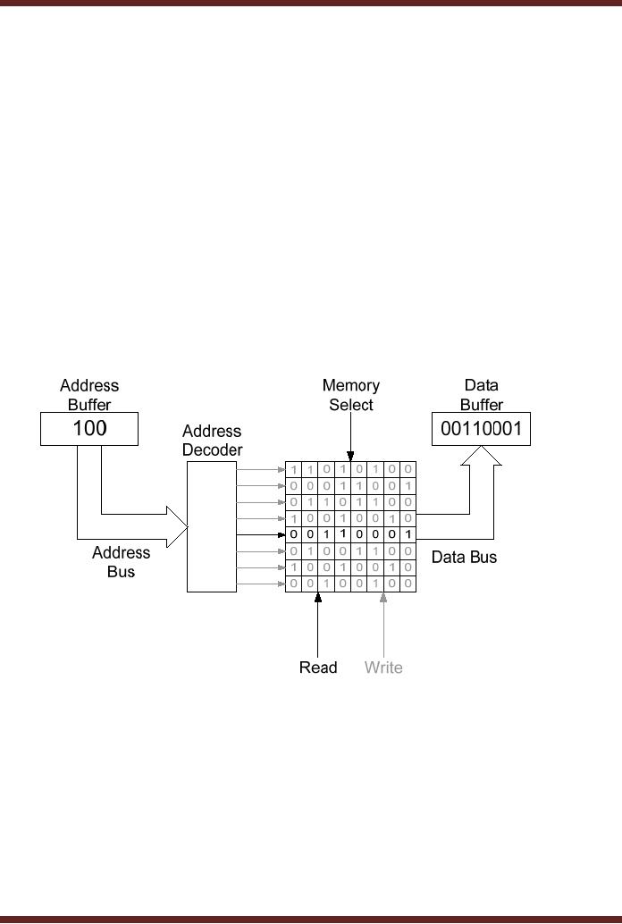
Memory Select signal. The
Read signal is asserted to
configure the memory
circuitry for
reading
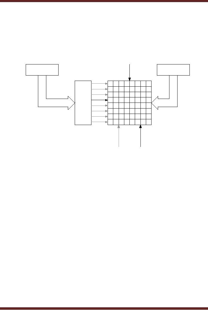
data from the memory. An
address (100) is applied on
the Address Lines. The
internal
address
decoder of the memory
decodes the address and
selects one unique row
from which
data is
read. Figure 39.4.
Figure
39.4 Memory Read
Operation
The
address of the location in
the memory from which
data is to be read is supplied
by
the
microprocessor. The microprocessor
stores the address in its
address buffer. The
data
read
from the memory is stored in
a data buffer inside the
microprocessor. In the
diagram
shown, a
microprocessor places an address
100 on its external address
bus connected to the
address
lines of the memory. The
internal address decoder of
the memory decodes
the
address
100 and activates a row
select line which selects
the row location 4. The
data
(00110001) at
the location is read from
the memory and placed on
the data bus where it
is
latched by
the microprocessor and
stored in its data
buffer.
Memory
Write operation
Memory
Write operation is carried
out by first selecting the
memory chip by
activating
the
Memory Select signal. The
Write signal is asserted to
configure the memory
circuitry for
397
CS302 -
Digital Logic & Design
writing
data to the memory. An
address (011) is placed on
the Address Lines by
the
microprocessor.
The internal address decoder
of the memory decodes the
address and
selects
one unique row select
line which selects the
row location 3. The data
(10110010) to be
written to
the selected memory location
is placed on the external
data bus by the
microprocessor
which is stored in the
selected location. Figure
39. 5
Memory
Address
Data
Select
Buffer
Buffer
011
10110010
Address
Decoder
1 1 0 1
0
1
00
0 00 1
1
0
0 1
0 1 1 0
1
1
00
1 0
1 01 1
0
0
00 1 1
0 1
0
0
Address
0 1 00 1
1
00
Data
Bus
1 0
1 00 1 0
0
Bus
00 1 00
00
1
Read
Write
Figure
39.5
Memory
Write Operation
Memory
Types
Two
major categories of memory
chips are the Random
Access Memory (RAM)
and
Read-Only
Memory (ROM). RAM allows a
read or write operation to be
carried out at any
address.
All locations are accessible
in equal time. RAM memories do
not store permanent
data. As
soon as the power supply to
the memory chip is turned
off, the entire data
stored in
the
memory is lost permanently. RAM
memories are also known as
volatile memories as
they
lose
data when the power is
turned off.
ROM chips
retain data permanently even
if the power to a ROM chip is
turned off.
ROM chips
are also known as
non-volatile memory chips
due to their ability to
retain data
permanently.
Since ROM chips are read
only, therefore user can
not write any information
to
ROM chips. ROM
chips are programmed by the
manufacturer and contain
important
information
which is required to start
(Boot Up) the
computer.
Random
Access Memory
(RAM)
RAM is divided
into two types, Static RAM
which uses flip-flops as
storage elements
and
Dynamic RAM which uses
capacitors to store binary
information. In a Static RAM
each
cell
which is capable of storing a
binary 0 or 1 is made up of a flip-flop
which retains
information as
long as power continues to be
supplied to the flip-flop.
Dynamic RAM on the
other
hand uses a capacitor to
store a single bit of data.
To store binary 1, the
capacitor is
charged
and to store binary 0, the
capacitor is in the uncharged
state. Capacitors over
a
period of
time lose their charge
and unless the Capacitors
are refreshed the
information stored
by the
capacitor is lost. Dynamic
memories periodically charge
their capacitors by
implementing a
Refresh cycle. Static
Memories are faster than
Dynamic memories
therefore
data
access in Static Memories is
faster as compared to Dynamic
Memories. Dynamic
398
CS302 -
Digital Logic & Design
memories on
the other hand have a
high density and can
store much more data
per unit area
and at a
lesser cost. Dynamic
memories have a high storage
density, as capacitors
are
simpler to
implement and occupy a very
small semiconductor area as
compared to flip-flops.
Static
RAM
Each
cell of a Static RAM is implemented
using a flip-flop which is
implemented using
several
MOSFET transistors. External
power is required to operate
the transistors. As long
as
the
external power is applied
the static memory cell
retains the data. The
circuit of a single
flip-
flop
based cell which can
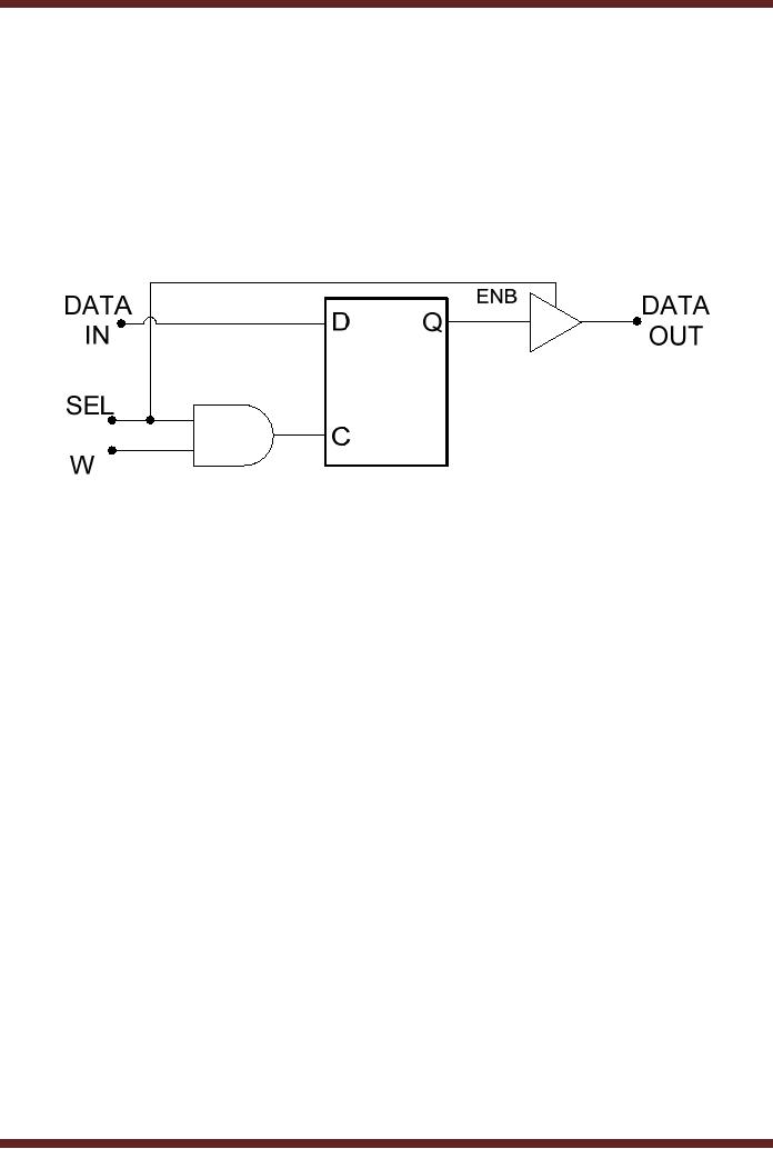
store a binary 0 or 1 is shown.
Figure 39.6.
Figure
39.6
Circuit
diagram of a Static Memory
Cell based on a
flip-flop
The
flip-flop used to store a
binary bit works like a
latch. When the SEL
signal is
activated,
the output buffer is enabled
allowing data to be read out
from the memory
cell.
When
both the SEL and
W(rite) signals are
activated the latch is
configured in the
transparent
mode
and the data applied at
the Data In line flows
through the latch to the
output. The Data In
and
Data Out lines can be
connected together to form a
bi-directional line which
does not
cause
any problems with the
reading or writing of data.
This is possible as the read
and write
operations
takes place at different
time intervals.
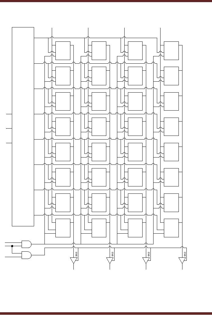
The
flip-flop based cells are
combined to form an array.
Additional logic is added
to
select
cells at appropriate locations
and to read and write
data. A 3 x 8 decoder decodes a
3-
bit
address to select any one of
the eight locations
comprising of a group of 4-cells.
For
example,
when the address is 000,
the first output line of
the 3 x 8 decoder is activated
which
is connected to
the SEL input of the
four latches in the first
row. Similarly, address
111
activates
the eighth output line of
the 3 x 8 decoder which
selects the four latches in
the last
row
(location). The memory array
has four Data In lines to
store the 4-bit data
values at the
eight
locations. Data In 3 and
Data In 0 represents the
most and least significant
bits of the 4-
bit
data respectively. The four
Data In lines connect the
Data In inputs of all the
latches in each
column
respectively. The memory
array also has four
Data Out lines, each
data line connects
the
output of each latch in a
column. The read and
write operations are
controlled through
the
three
signals W, CS and OE. The
Chip Select (CS) signal
along with the Output
Enable (OE)
signal
enable each of the four
tri-state buffers connected to
end of each Data Out
line. When
data is to be
read from a memory array,
the memory chip is selected
and the output
enabled.
The
Write (W) signal along
with the CS signal are
used to write data into
any 4-bit location.
Figure
39.7.
To write
data 1001 at the 6th memory location, the
address A2, A1 and A0
bits
are set to
110
which select the 6th row of the memory
array. The data 1001 is
placed at the four Data
In
lines
respectively. The CS and W
signals are activated which
set the four latches in
the sixth
399

CS302 -
Digital Logic & Design
row to
transparent mode allowing
data 1001 applied at the
four Data In lines to be
available at
the Q
outputs of the four latches
respectively. As soon as the CS
and W signals are
deactivated,
the latches store the
data value.
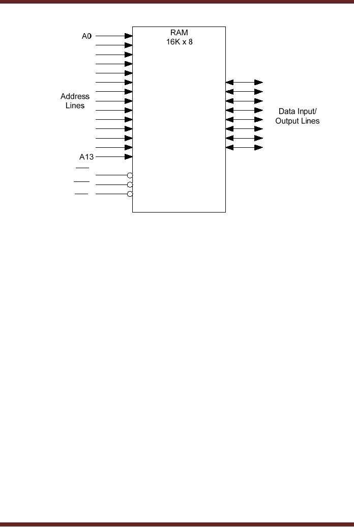
A 16K x 8
memory is shown. Figure
39.8. The memory is capable
of storing byte
values in 16 x
1024 locations. To address
these unique locations,
fourteen address lines
are
required.
The memory has eight
bi-directional data lines
through which data is
read/written at
selected
memory locations. The three
CS, WE and OE are shown to
be active low.
400
CS302 -
Digital Logic & Design
DATA
IN
DATA
IN
DATA
IN
DATA
IN
3x8
2
0
3
1
Decoder
IN
OUT
IN
OUT
IN
OUT
IN
OUT
SEL
SEL
SEL
SEL
WR
WR
WR
WR
IN
OUT
IN
OUT
IN
OUT
IN
OUT
SEL
SEL
SEL
SEL
WR
WR
WR
WR
IN
OUT
IN
OUT
IN
OUT
IN
OUT
SEL
SEL
SEL
SEL
WR
WR
WR
WR
A2
IN
OUT
IN
OUT
IN
OUT
IN
OUT
A1
SEL
SEL
SEL
SEL
WR
WR
WR
WR
A0
IN
OUT
IN
OUT
IN
OUT
IN
OUT
SEL
SEL
SEL
SEL
WR
WR
WR
WR
IN
OUT
IN
OUT
IN
OUT
IN
OUT
SEL
SEL
SEL
SEL
WR
WR
WR
WR
IN
OUT
IN
OUT
IN
OUT
IN
OUT
SEL
SEL
SEL
SEL
WR
WR
WR
WR
IN
OUT
IN
OUT
IN
OUT
IN
OUT
SEL
SEL
SEL
SEL
WR
WR
WR
WR
W
CS
OE
DATA
OUT
DATA
OUT
DATA
OUT
DATA
OUT
3
2
1
0
Figure
39.7 Internal Structure of a 8 x 4
Static RAM
401
CS302 -
Digital Logic & Design
CS
WE
OE
Figure
39. 8
16K x 8
Static RAM
402
Table of Contents:
- AN OVERVIEW & NUMBER SYSTEMS
- Binary to Decimal to Binary conversion, Binary Arithmetic, 1’s & 2’s complement
- Range of Numbers and Overflow, Floating-Point, Hexadecimal Numbers
- Octal Numbers, Octal to Binary Decimal to Octal Conversion
- LOGIC GATES: AND Gate, OR Gate, NOT Gate, NAND Gate
- AND OR NAND XOR XNOR Gate Implementation and Applications
- DC Supply Voltage, TTL Logic Levels, Noise Margin, Power Dissipation
- Boolean Addition, Multiplication, Commutative Law, Associative Law, Distributive Law, Demorgan’s Theorems
- Simplification of Boolean Expression, Standard POS form, Minterms and Maxterms
- KARNAUGH MAP, Mapping a non-standard SOP Expression
- Converting between POS and SOP using the K-map
- COMPARATOR: Quine-McCluskey Simplification Method
- ODD-PRIME NUMBER DETECTOR, Combinational Circuit Implementation
- IMPLEMENTATION OF AN ODD-PARITY GENERATOR CIRCUIT
- BCD ADDER: 2-digit BCD Adder, A 4-bit Adder Subtracter Unit
- 16-BIT ALU, MSI 4-bit Comparator, Decoders
- BCD to 7-Segment Decoder, Decimal-to-BCD Encoder
- 2-INPUT 4-BIT MULTIPLEXER, 8, 16-Input Multiplexer, Logic Function Generator
- Applications of Demultiplexer, PROM, PLA, PAL, GAL
- OLMC Combinational Mode, Tri-State Buffers, The GAL16V8, Introduction to ABEL
- OLMC for GAL16V8, Tri-state Buffer and OLMC output pin
- Implementation of Quad MUX, Latches and Flip-Flops
- APPLICATION OF S-R LATCH, Edge-Triggered D Flip-Flop, J-K Flip-flop
- Data Storage using D-flip-flop, Synchronizing Asynchronous inputs using D flip-flop
- Dual Positive-Edge triggered D flip-flop, J-K flip-flop, Master-Slave Flip-Flops
- THE 555 TIMER: Race Conditions, Asynchronous, Ripple Counters
- Down Counter with truncated sequence, 4-bit Synchronous Decade Counter
- Mod-n Synchronous Counter, Cascading Counters, Up-Down Counter
- Integrated Circuit Up Down Decade Counter Design and Applications
- DIGITAL CLOCK: Clocked Synchronous State Machines
- NEXT-STATE TABLE: Flip-flop Transition Table, Karnaugh Maps
- D FLIP-FLOP BASED IMPLEMENTATION
- Moore Machine State Diagram, Mealy Machine State Diagram, Karnaugh Maps
- SHIFT REGISTERS: Serial In/Shift Left,Right/Serial Out Operation
- APPLICATIONS OF SHIFT REGISTERS: Serial-to-Parallel Converter
- Elevator Control System: Elevator State Diagram, State Table, Input and Output Signals, Input Latches
- Traffic Signal Control System: Switching of Traffic Lights, Inputs and Outputs, State Machine
- Traffic Signal Control System: EQUATION DEFINITION
- Memory Organization, Capacity, Density, Signals and Basic Operations, Read, Write, Address, data Signals
- Memory Read, Write Cycle, Synchronous Burst SRAM, Dynamic RAM
- Burst, Distributed Refresh, Types of DRAMs, ROM Read-Only Memory, Mask ROM
- First In-First Out (FIFO) Memory
- LAST IN-FIRST OUT (LIFO) MEMORY
- THE LOGIC BLOCK: Analogue to Digital Conversion, Logic Element, Look-Up Table
- SUCCESSIVE –APPROXIMATION ANALOGUE TO DIGITAL CONVERTER