 |
CS302 -
Digital Logic & Design
Lesson
No. 35
APPLICATIONS OF
SHIFT REGISTERS
The
major application of a shift
register is to convert between
parallel and serial
data.
Shift
registers are also used as
keyboard encoders. The two
applications of the shift
registers
are
discussed.
1.
Serial-to-Parallel Converter
Earlier,
Multiplexer and Demultiplexer
based Parallel to Serial and
Serial to Parallel
converters
were discussed. The
Multiplexer and Demultiplexer
require registers to store
the
parallel
data that is converted into
serial data and parallel
data which is obtained
after
converting
the incoming serial data. A
Parallel In/Serial Out shift
register offers a
better
solution
instead of using a Multiplexer-Register
combination to convert parallel
data into serial
data.
Similarly, a Serial In/Parallel
Out shift register replaces
a Demultiplexer-Register
combination.
In Asynchronous
Serial data transmission
mode, a character which is
constituted of 8-
bits
(which can include a parity
bit) is transmitted. To separate
one character from another
and
to indicate
when data is being
transmitted and when the
serial transmission line is
idle (no data
is being
transmitted) a set of start
bit and stop bits
are appended at both ends of
the 8-bit
character. A
character is preceded by a logic
low start bit. When
the line is idle it is set
to logic
high,
when a character is about to be
transmitted the start bit
sets the line to logic
low. The
logic
low start bit is an
indication that 8 character
bits are to follow and
the transmission line
is
no longer in an
idle state. After
8-character bits have been
transmitted, the end of
the
character is
indicated by two stop bits
that are at logic high.
The two logic bits
indicate the end
of the
character and also set
the transmission line to the
idle state. Therefore a
total of 11 bits
are
transmitted to send one
character from one end to
the other. The logic
low start bit is
also
a signal
for the receiver circuit to
start receiving the 8
character bits that are
following the start
bit.
The 11-bit serial character
format is shown. Figure
35.1.
0
0/1
0/1
0/1
0/1
0/1
0/1
0/1
0/1
1
1
Stop
Data
bits
Stop
bits
bit
Figure
35.1
11-bit
Serial Data format
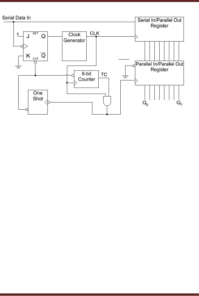
A Serial to
Parallel converter circuit
based on shift registers is
shown. Figure 35.2.
The
serial
data is preceded by a logic
low start bit which
triggers the J-K flip-flop.
The output of the
flip-flop is
set to logic high which
enables the clock generator.
The clock pulses generated
are
connected to
the clock input of a Serial
In/Parallel Out shift
register and also to the
clock input
of an 8-bit
counter. On each clock
transition, the Serial
In/Parallel Out shift
register shifts in
one
bit data. When the
8-bit counter reaches its
terminal count 111, the
terminal count output
signal
along with the clock
signal trigger the One-Shot
and also allow the
Parallel In/Parallel
Out
register to latch in the
Parallel data at the output
of the Serial In/Parallel
Out shift register.
The
One-shot resets the J-K
flip-flop output Q to logic 0
disabling the clock
generator and also
clears
the 8-bit counter to count
000.
356
CS302 -
Digital Logic & Design
LOAD
Figure
35.2
Series-to-Parallel
Converter
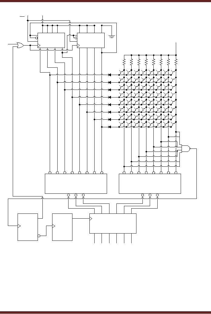
2. Keyboard
Encoder
Earlier a
simple keypad encoder
circuit was discussed where,
the 0 to 9 digit
keypad
was
connected through a decade to
BCD encoder. Pressing any
keypad key enables
the
corresponding
input of the encoder circuit
which encodes the input as a
4-bit BCD output.
Computer
keyboards which have more
keys employ a keyboard
encoder circuit that
regularly
scans
the keyboard to check for
any key press. Figure
35.3. The scanning is done
by
organizing
the keys in the form of
rows and columns. With
the help of a shift register
based
ring
counter one row is selected
at a time. The two counters
are connected as an 8-bit
Ring
counter
which sequences through a
bit pattern having all
1's and a single 0. The 8
state
sequence
selects one row at a time by
setting it to logic 0. If a key is
pressed, the
corresponding
column also becomes logic 0
as it connected to the selected
row. The row
and
column
which are selected are
encoded by the row and
column encoders. When a key
is
pressed,
the selected column which is
set to logic 0 sets the
output of the NAND gate to
logic
1 which
triggers two One Shots.
The first One Shot
inhibits the clock signal to
the ring counters
for a
short interval until the
Key Code is stored. The
One Shot also triggers
the second One-
Shot
that sends a pulse to the
clock input of the Key
Code register. The Key
Code Register
stores
the key ID represented as
3-bit column and 3-bit
row code.
357
CS302 -
Digital Logic & Design
+V
SH / LD
CLK
74HC195
74HC195
(5KHz)
+V
Row
Encoder
Column
Encoder
74HC147
74HC147
One
One
Key
Code Register
Shot
Shot
74HC174A
Figure
35.3
Keyboard
Encoder circuit
Programmable
Sequential Logic
Earlier
PLD devices were discussed
and their Combinational
Modes were discussed.
PLD
devices can be programmed to
implement Sequential Circuits.
The AND-OR gate array
of
a PLD
device is used to implement
the excitation inputs for
the memory element. The
Memory
element is
implemented in the form of a
flip-flop in each OLMC
module of the PLD device.
The
present
state output of the memory
element is connected back to
the AND gate array to
form
358
CS302 -
Digital Logic & Design
the
input combinational circuit
that generates the
excitation inputs for the
memory element.
The
output of the sequential
circuit is obtained from the
tri-state buffer which
connects the
output of
the OLMC module to the
output pin of the PLD
device. The output of the
tri-state
buffer is
determined by the current
state of the flip-flop and
the combinational external
input
which is
connected to the control
input of the tri-state
buffer which enables or
disables the tri-
state
buffer output.
The
Registered Mode
In the
discussion on Combinational Logic
with PLDs, the two
active-low and
active-high
Combinational
Modes of the PLD device
were discussed. In Sequential
Logic with PLD
devices
the Registered Active-low
and Active high Modes
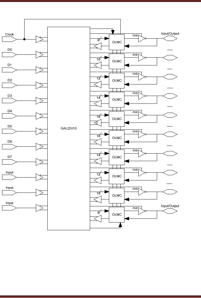
are used. Figure
35.4
Figure
35.4
OLMC of
the GAL22V10 device
The
PLD is selected for
Sequential operation by configuring
the OLMC in the
Registered
Mode by setting the 1-to-4
MUX select inputs S1 and S0 to 01 or
00. By setting the
MUX select
inputs S1 and S0 to 01 respectively,
the Q output of the D
flip-flop is made
available at
the out of the Multiplexer
which is connected to the
output tri-state buffer. The
S1
select
input of the 1-to-2 MUX is
also set to 0 in the
Registered Mode operation,
which allows
the Q output of the D flip-flop to
be feed back to the AND gate
array. In the Registered
Mode
the
feedback from the tri-state
buffer output can not be
used as a feedback to the AND
gate
array. By
setting the S1 and S0 select
inputs of the 1-to-4 MUX to 00
respectively, the
output
of the MUX is
connected to the Q output of the D flip-flop
instead of the Q output.
The
feedback to
the AND gate array however
remains the same, which is
connected to the
Q output of the D
flip-flop.
Software
Mode Specification
The
Combinational or Registered Modes of
the OLMC are selected by
programming
statements in
the declaration part of the
input file and the
way logic descriptions are
written.
The
ISTYPE statement is used in
the declaration part with
the statements assigning
PIN
numbers to
output variables.
X
PIN 22
ISTYPE
`reg';
Y
PIN 23
ISTYPE
`com';
Figure
35.5a ISTYPE statement to
declare an input as Registered or
Combinational
359

CS302 -
Digital Logic & Design
The
declaration statements describe
variable X and Y available at
output pins 22 and 23
respectively.
The X variable is a `Registered'
output available from the
D-flip-flop. The Y
variable is a
`Combinational' output available
directly from the AND-OR
gate array output.
The
active-low or
active-high output of the
Registered Mode can also be
specified in the
declaration
statement
X
PIN 22
ISTYPE
`reg.buffer;
Z
PIN 20
ISTYPE
`reg.invert';
Figure
35.5b ISTYPE statement to
specifying active-high or active-low
Registered Mode
output
The
first declaration statement
describes X output variable as an
active-high Registered
Mode
output.
The second statement
describes Z output variable as an
active-low Registered
Mode
output.
The
assignment operators `:='
and `:>' are used in
logic descriptions to indicate a
Registered
output.
X := D;
Y = D;
Figure
35.5c Assignment Operators
for Registered Mode
The
first logical declaration
statement indicates that X
will be assigned the value
of D on the
clock
transition and will hold
the value until the
next clock transition. The
second logical
declaration
indicates that output Y is
equal to input D.
The
dot extension `.CLK' is used
to indicate that the
register device is a clocked
flip-flop. A
statement
using the dot extension
must accompany a logical
declaration statement.
X := D;
X.CLK =
Clock;
Figure
35.5d Dot assignment to
indicate clocked
flip-flop
Example1:
Parallel Input/Parallel Output
8-bit Register with inverted
outputs
A PLD
device such as GAL22V10 can
be programmed to work as an 8-bit D
flip-flop
based
register with inverted
outputs. The ABEL statements
for configuring the PLD
are shown.
Figure
35.6
The
pin declarations are
Clock,
D0, D1, D2, D3,
D4, D5, D6 D7
PIN
1, 2, 3, 4, 5, 6, 7, 8,
9;
Q0,
Q1, Q2, Q3, Q4,
Q5, Q6, Q7
PIN
22,
21, 20, 19, 18,
17, 16, 15
ISTYPE
`reg.invert';
The
logical declarations
are
[Q0,
Q1, Q2, Q3, Q4,
Q5, Q6, Q7] := [D0,
D1, D2, D3, D4,
D5, D6, D7];
[Q0,
Q1, Q2, Q3, Q4,
Q5, Q6, Q7].CLK =
Clock;
360

CS302 -
Digital Logic & Design
The
logical declarations can
also be written as
Q0 :=
D0;
Q0.CLK =
Clock;
Q1 :=
D1;
Q1.CLK =
Clock;
Q2 :=
D2;
Q2.CLK =
Clock;
Q3 :=
D3;
Q3.CLK =
Clock;
Q4 :=
D4;
Q4.CLK =
Clock;
Q5 :=
D5;
Q5.CLK =
Clock;
Q6 :=
D6;
Q6.CLK =
Clock;
Q7 :=
D7;
Q7.CLK =
Clock;
Figure
35.6a ABEL Statements for
implementing an 8-bit register
with inverted outputs
361
CS302 -
Digital Logic & Design
Q0
Q1
Q2
Q3
Q4
Q5
Q6
Q7
Figure
35.6b GAL22V10 configured as an
8-bit inverted output
register
Example2:
8-bit Serial In/Parallel Out
Shift Register
An 8-bit
Serial In/Parallel out shift
register based on an identical D
type flip-flop is
shown.
Figure 35.7. The Clear
signal has to be set to
logic 0 to asynchronously clear
all the
flip-flops.
The Enable input has to be
set to logic 1 to allow
serial data to be shifted
in. An 8-bit
Serial
In/Parallel Out Shift
Register is implemented using
the GAL22V10 PLD. The D
flip-flop
implemented in
the OLMC is triggered on the
positive clock edge. It also
has active-high,
asynchronous
set and clear
inputs.
362
CS302 -
Digital Logic & Design
Figure
35.7
8-bit
Serial In/Parallel Out Shift
Register
Module
Right_bit_shift_register
Title
`8-bit shift register in a
GAL22V10'
"Device
Declaration
Register
Device
`P22V10'
"Pin
Declaration
Clock,
Clear
Pin 1,
2;
Data,
Enable
Pin 3,
4;
Q0,
Q1, Q2, Q3, Q4,
Q5, Q6, Q7
Pin
16, 17, 18, 19,
20, 21, 22, 23
ISTYPE
`reg.buffer';
Equations
Q0 := Data &
Enable;
[Q1,
Q2, Q3, Q4, Q5,
Q6, Q7] := [Q0, Q1,
Q2, Q3, Q4, Q5,
Q6];
[Q0,
Q1, Q2, Q3, Q4,
Q5, Q6, Q7].CLK =
clock;
[Q0,
Q1, Q2, Q3, Q4,
Q5, Q6, Q7].AR =
!clear;
Test_Vectors
([Clock,
Clear, Data, Enable] ->
[Q0, Q1, Q2, Q3,
Q4, Q5, Q6,
Q7])
[ .x. , 0
, .x. , .x. ] -> [0 , 0 , 0 , 0 , 0 , 0
, 0 , 0 ];
[ .c. , 1
, 1 ,
0 ] -> [0 , 0 , 0 ,
0 , 0 , 0 , 0 , 0 ];
[ .c. , 1
, 0 ,
1 ] -> [0 , 0 , 0 ,
0 , 0 , 0 , 0 , 0 ];
[ .c. , 1
, 1 ,
1 ] -> [1 , 0 , 0 ,
0 , 0 , 0 , 0 , 0 ];
[ .c. , 1
, 0 ,
1 ] -> [0 , 1 , 0 ,
0 , 0 , 0 , 0 , 0 ];
[ .c. , 1
, 1 ,
1 ] -> [1 , 0 , 1 ,
0 , 0 , 0 , 0 , 0 ];
[ .c. , 1
, 0 ,
1 ] -> [0 , 1 , 0 ,
1 , 0 , 0 , 0 , 0 ];
[ .c. , 1
, 1 ,
1 ] -> [1 , 0 , 1 ,
0 , 1 , 0 , 0 , 0 ];
[ .c. , 1
, 0 ,
1 ] -> [0 , 1 , 0 ,
1 , 0 , 1 , 0 , 0 ];
[ .c. , 1
, 1 ,
1 ] -> [1 , 0 , 1 ,
0 , 1 , 0 , 1 , 0 ];
[ .c. , 1
, 0 ,
1 ] -> [0 , 1 , 0 ,
1 , 0 , 1 , 0 , 1 ];
[ .c. , 1
, 1 ,
1 ] -> [1 , 0 , 1 ,
0 , 1 , 0 , 1 , 0 ];
[ .c. , 0
, 1 ,
1 ] -> [0 , 0 , 0 ,
0 , 0 , 0 , 0 , 0 ];
END
Figure
35.8
ABEL
Input file for Serial
In/Parallel Out Shift
register
363

CS302 -
Digital Logic & Design
The
ABEL Input file format
for the shift register is
shown in figure 35.4. The
Equations
and
the Test_Vectors declarations
are,
�
Q0 := Data &
Enable;
The Q0
output is active high and
depends upon the product of
Data input and the
Enable
input
and Q0 will be assigned the
product value at the
positive transition of the
clock.
�
[Q1,
Q2, Q3, Q4, Q5,
Q6, Q7] := [Q0, Q1,
Q2, Q3, Q4, Q5,
Q6];
[Q0,
Q1, Q2, Q3, Q4,
Q5, Q6, Q7].CLK =
Clock;
The
Q0, Q1, Q2, Q3,
Q4, Q5, Q6 outputs are
assigned to Q1, Q2, Q3,
Q4, Q5, Q6, Q7
respectively on
a clock transition.
�
[Q0,
Q1, Q2, Q3, Q4,
Q5, Q6, Q7].AR =
!Clear;
The
Q0, Q1, Q2, Q3,
Q4, Q5, Q6, Q7 outputs
are reset on a Clear signal applied at
the
Asynchronous
Reset (AR) Input.
�
([Clock,
Clear, Data, Enable] ->
[Q0, Q1, Q2, Q3,
Q4, Q5, Q6,
Q7])
[ .x. , 0
, .x. , .x. ] -> [0 , 0 , 0 , 0 , 0 , 0
, 0 , 0 ];
[ .c. , 1
, 1 ,
0 ] -> [0 , 0 , 0 ,
0 , 0 , 0 , 0 , 0 ];
[ .c. , 1
, 0 ,
1 ] -> [0 , 0 , 0 ,
0 , 0 , 0 , 0 , 0 ];
[ .c. , 1
, 1 ,
1 ] -> [1 , 0 , 0 ,
0 , 0 , 0 , 0 , 0 ];
The
Test_Vector specifies `x' as
don't care, `c' as clock
signal, thus the first
vector specifies
logic 0
outputs when Clear input is
logic 0. Clock, Data and
Enable inputs are don't
care.
The
second vector specifies a
clock transition with,
Clear, Data and Enable
inputs set to
logic 1, 1
and 0 respectively. The
Enable input is set to logic
0 therefore the shift
operation
is inhibited.
The third vector enables
the shift operation with
logic 0 shifted in. The
fourth
vector
shifts in logic 1.
Example3:
4-bit Parallel In/Serial Out
Shift Register
A 4-bit
Parallel In/Serial Out shift
register is shown. Figure
35.9. It is very similar to
the
register
discussed earlier, except
that the shift register
shown has an asynchronous
reset input
which
clears the shift register.
The ABEL Input file
for the 4-bit Parallel
In/Serial Out shift
register is
shown in figure
35.10.
364
CS302 -
Digital Logic & Design
D0
D1
D2
D3
SHIFT /
LOAD
1
2
1
2
1
2
Q3
SET
SET
SET
SET
D
D
D
D
Q
Q
Q
Q
Q0
Q1
Q2
Serial
Data
flip-flop
1
flip-flop
2
flip-flop
3
flip-flop
4
Out
Q
Q
Q
Q
CLR
CLR
CLR
CLR
CLK
Clear
Figure
35.9
4-bit
Parallel In/Serial Out Shift
Register
Module
Four_bit_shift_register
Title
`4-bit shift register in a
GAL22V10'
"Device
Declaration
Register
Device
`P22V10'
"Pin
Declaration
Clock,
Clear
Pin 1,
2;
SHLD
Pin
3;
D0,
D1, D2, D3
Pin 4, 5, 6, 7
ISTYPE `reg.buffer';
Q0,
Q1, Q2, Q3
Pin
14, 15, 16, 17 ISTYPE
`reg.buffer';
Equations
Q0 :=
D0;
Q1 := Q0 &
SHLD # D1 & !SHLD;
Q2 := Q1 &
SHLD # D2 & !SHLD;
Q3 := Q2 &
SHLD # D3 & !SHLD;
[Q0,
Q1, Q2, Q3].CLK =
clock;
[Q0,
Q1, Q2, Q3].AR =
!clear;
Test_Vectors
([Clock,
Clear, SHLD, D0, D1,
D2, D3] -> [Q3])
[ .x. , 0
, .x. , .x. , .x. ,
.x. , .x. ] -> [ 0 ];
365

CS302 -
Digital Logic & Design
[
.c.
,
1
,
0
,
0
,
1
,
0,
1 ] -> [ 1
];
[
.c.
,
1
,
0
,
1
,
0
,
1,
0 ] -> [ 0
];
[
.c.
,
1
,
1
,
1
,
0
,
1,
0 ] -> [ 1
];
[
.c.
,
1
,
1
,
1
,
0
,
1,
0 ] -> [ 0
];
[
.c.
,
1
,
1
,
1
,
0
,
1,
0 ] -> [ 1
];
[
.c.
,
0
,
0
,
1
,
0
,
1,
0 ] -> [ 0
];
END
Figure
35.10 ABEL Input file
for a 4-bit Parallel
In/Serial Out Shift
register
The
Equations and the
Test_Vectors declarations
are,
� Q0 :=
D0;
The Q0
output is active high and is
assigned the value Do at the
positive transition of
the
clock.
�
Q1 := Q0 &
SHLD # D1 & !SHLD;
Q2 := Q1 &
SHLD # D2 & !SHLD;
Q3 := Q2 &
SHLD # D3 & !SHLD;
[Q0,
Q1, Q2, Q3].CLK =
clock;
The
Q1, Q2 and Q3 output is
assigned the value based on
the Boolean
expression
Q0.SHLD
+
D1.SHLD
, Q1.SHLD
+
D2.SHLD
and Q2.SHLD
+
D3.SHLD
on a
positive
clock
transition.
�
[Q0,
Q1, Q2, Q3].AR =
!clear;
The
Q0, Q1, Q2, Q3 outputs
are reset on a Clear signal applied at the
Asynchronous
Reset
(AR) Input.
�
([Clock,
Clear, SHLD, D0, D1,
D2, D3] -> [Q3])
[ .x. , 0
, .x. , .x. , .x. ,
.x. , .x. ] -> [ 0 ];
[ .c. , 1
, 0 , 0 , 1 , 0 , 1 ] -> [ 1 ];
The
Test_Vector specifies `x' as
don't care, `c' as clock
signal, thus the first
vector specifies
logic 0
output at Q3 when Clear
input is logic 0. Clock,
SHLD, D0, D1, D2 and D3
inputs
are
don't care. The second
vector specifies a clock
transition with, Clear,
SHLD, D0, D1,
D2 and D3
inputs set to logic 1, 0, 0, 1, 0
and 1 respectively. The data
0101 is loaded into
the
register with the Q3 output
set to 1.
366
Table of Contents:
- AN OVERVIEW & NUMBER SYSTEMS
- Binary to Decimal to Binary conversion, Binary Arithmetic, 1’s & 2’s complement
- Range of Numbers and Overflow, Floating-Point, Hexadecimal Numbers
- Octal Numbers, Octal to Binary Decimal to Octal Conversion
- LOGIC GATES: AND Gate, OR Gate, NOT Gate, NAND Gate
- AND OR NAND XOR XNOR Gate Implementation and Applications
- DC Supply Voltage, TTL Logic Levels, Noise Margin, Power Dissipation
- Boolean Addition, Multiplication, Commutative Law, Associative Law, Distributive Law, Demorgan’s Theorems
- Simplification of Boolean Expression, Standard POS form, Minterms and Maxterms
- KARNAUGH MAP, Mapping a non-standard SOP Expression
- Converting between POS and SOP using the K-map
- COMPARATOR: Quine-McCluskey Simplification Method
- ODD-PRIME NUMBER DETECTOR, Combinational Circuit Implementation
- IMPLEMENTATION OF AN ODD-PARITY GENERATOR CIRCUIT
- BCD ADDER: 2-digit BCD Adder, A 4-bit Adder Subtracter Unit
- 16-BIT ALU, MSI 4-bit Comparator, Decoders
- BCD to 7-Segment Decoder, Decimal-to-BCD Encoder
- 2-INPUT 4-BIT MULTIPLEXER, 8, 16-Input Multiplexer, Logic Function Generator
- Applications of Demultiplexer, PROM, PLA, PAL, GAL
- OLMC Combinational Mode, Tri-State Buffers, The GAL16V8, Introduction to ABEL
- OLMC for GAL16V8, Tri-state Buffer and OLMC output pin
- Implementation of Quad MUX, Latches and Flip-Flops
- APPLICATION OF S-R LATCH, Edge-Triggered D Flip-Flop, J-K Flip-flop
- Data Storage using D-flip-flop, Synchronizing Asynchronous inputs using D flip-flop
- Dual Positive-Edge triggered D flip-flop, J-K flip-flop, Master-Slave Flip-Flops
- THE 555 TIMER: Race Conditions, Asynchronous, Ripple Counters
- Down Counter with truncated sequence, 4-bit Synchronous Decade Counter
- Mod-n Synchronous Counter, Cascading Counters, Up-Down Counter
- Integrated Circuit Up Down Decade Counter Design and Applications
- DIGITAL CLOCK: Clocked Synchronous State Machines
- NEXT-STATE TABLE: Flip-flop Transition Table, Karnaugh Maps
- D FLIP-FLOP BASED IMPLEMENTATION
- Moore Machine State Diagram, Mealy Machine State Diagram, Karnaugh Maps
- SHIFT REGISTERS: Serial In/Shift Left,Right/Serial Out Operation
- APPLICATIONS OF SHIFT REGISTERS: Serial-to-Parallel Converter
- Elevator Control System: Elevator State Diagram, State Table, Input and Output Signals, Input Latches
- Traffic Signal Control System: Switching of Traffic Lights, Inputs and Outputs, State Machine
- Traffic Signal Control System: EQUATION DEFINITION
- Memory Organization, Capacity, Density, Signals and Basic Operations, Read, Write, Address, data Signals
- Memory Read, Write Cycle, Synchronous Burst SRAM, Dynamic RAM
- Burst, Distributed Refresh, Types of DRAMs, ROM Read-Only Memory, Mask ROM
- First In-First Out (FIFO) Memory
- LAST IN-FIRST OUT (LIFO) MEMORY
- THE LOGIC BLOCK: Analogue to Digital Conversion, Logic Element, Look-Up Table
- SUCCESSIVE –APPROXIMATION ANALOGUE TO DIGITAL CONVERTER