 |
CS302 -
Digital Logic & Design
Lesson
No. 34
SHIFT
REGISTERS
The
need to storage binary data
was discussed earlier. In
digital circuits multi-bit
data
has to be
stored temporarily until it is
processed. A flip-flop is able to
store a single binary bit
of
information.
Multiple bits of data are
stored by using multiple
flip-flops which have their
clock
inputs
connected together. Thus, by
activating the clock signal
multiple-bits of data are
stored.
Technically, a
register performs two basic
functions. It stores data
and it moves or
shifts
data. The shifting of data
involves shifting of bits
from one flip-flop to the
other within the
register or
moving data in and out of
the register. The shift
operation of the binary data
is
carried
out by applying clock
signals. Several different
kinds of shift operations
can be
identified.
The different shift
operations are described
using a 4-bit shift
register.
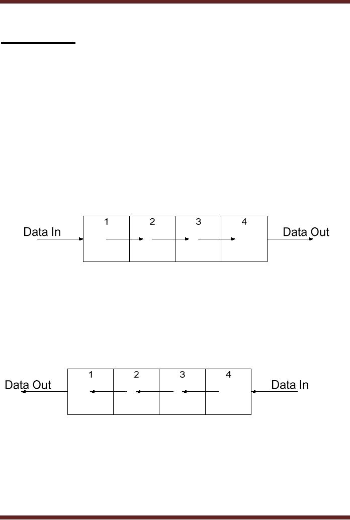
1. Serial
In/Shift Right/Serial Out
Operation
Data is
shifted in the right-hand
direction one bit at a time
with each transition of
the
clock
signal. Figure 34.1. The
data enters the shift
register serially from the
left hand side
and
after
four clock transitions the
4-bit register has 4-bits of
data. The data is shifted
out serially
one
bit at a time from the
right hand side of the
register if clock signals
are continuously
applied.
Thus after 8 clock signals
the 4-bit data is completely
shifted out of the shift
register.
Figure
34.1
Serial
In/Serial Right/Serial Out
Operation
2. Serial
In/Shift Left/Serial Out
Operation
Data is
shifted in the left-hand
direction one bit at a time
with each transition of
the
clock
signal. Figure 34.2. The
data enters the shift
register serially from the
right hand side
and
after
four clock transitions the
4-bit register has 4-bits of
data. The data is shifted
out serially
one
bit at a time from the
left hand side of the
register if clock signals
are continuously
applied.
Thus
after 8 clock signals the
4-bit data is completely
shifted out of the shift
register.
Figure
34.2
Serial
In/Serial Left/Serial Out
Operation
The
Serial Shift register has
been discussed earlier,
implemented using J-K
flip-flops.
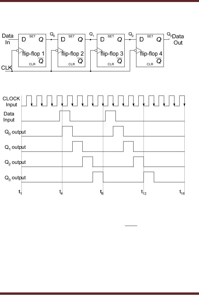
Serial
shift registers can be
implemented using any type
of flip-flops. A serial shift
register
implemented
using D flip-flops with the
serial data applied at the D
input of the first flip-flop
and
serial
data out obtained at the Q
output of the last flip-flop
is shown. Figure 34.3. At
each clock
transition
1bit of serial data is
shifted in and at the same
instant 1-bit of serial data
is shifted
out.
For a 4-bit shift register,
8 clock transitions are
required to shift in 4-bit
data and
346
CS302 -
Digital Logic & Design
completely
shift out the 4-bit
data. As the data is shifted
out 1-bit at a time, a logic
0 value is
usually
shifted in to fill up the
vacant bits in the shift
register.
Figure
34.3a Serial In/Shift
Right/Serial Out
Register
Figure
34.3b Timing diagram of a
Serial In/Shift Right/Serial
Out Register
The
shift left and shift
right shift registers are
identical in their working.
They are
connected
differently for shift left
and shift right operations.
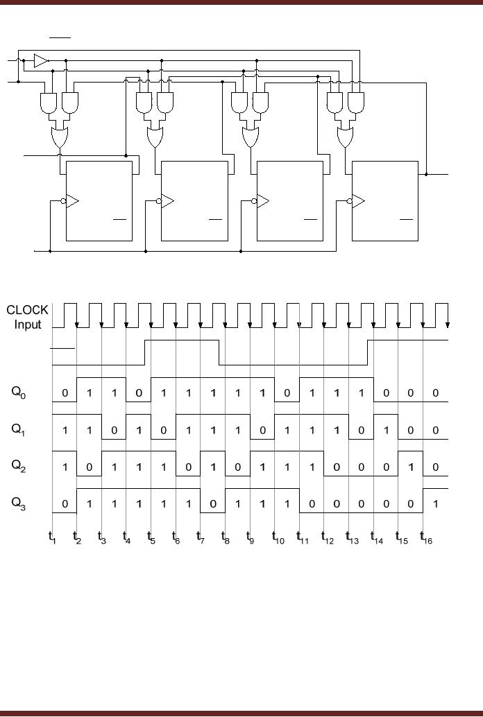
Bidirectional Shift Registers
are
available
which allow data to be
shifted left or right.
Figure 34.4. The 4-bit
register is
configured to
shift left or right by
setting the RIGHT / LEFT signal to logic high or
low
respectively.
When the register is
configured to shift right,
the AND gates marked 1
are
enabled.
The input of the first
flip-flop is connected to the
serial Input, the inputs of
the next
three
flip-flops are connected to
the Q outputs of the
previous flip-flops. Thus on a
clock
transition
data is shifted 1-bit
towards the right. The
serial data is shifted out
of the register
through
output Q3. When
the register is configured to
shift left the AND gates
marked 2 are
enabled,
connecting the Q outputs of
the flip-flop on the right
hand side to the D input of
the
flip-flop on
the left hand side.
Thus on each clock
transition data is shifted
1-bit towards left.
Serial
date out is available
through the Q0 output. Serial data is
input through the Serial
Data in
line
which is connected to the
fourth AND gate marked 2 on
the extreme right hand
side.
347
CS302 -
Digital Logic & Design
RIGHT /
LEFT
Serial
1
2
1
2
1
2
1
2
Data
In
Q0
Q3
SET
SET
SET
SET
D
D
D
D
Q
Q
Q
Q
Q0
Q1
Q2
flip-flop
1
flip-flop
2
flip-flop
3
flip-flop
4
Q
Q
Q
Q
CLR
CLR
CLR
CLR
CLK
Figure
34.4a Bi-directional, 4-bit
Shift register
RIGHT /
LEFT
Figure
34.4b Timing diagram of a
Bi-directional, 4-bit Shift
register
The
timing diagram shows the
operation the Bi-directional
shift register which
initially shifts
data
towards the left. At
interval t5,
the registered is configured to
shift right and at t8 towards
left
and again towards the
right at interval t14. A
logic 1 is applied at the
Serial data input
from
intervals
t1 to t10. At
interval t11
and
onwards a logic 0 is applied at
the Serial data
input.
3. Serial
In/Parallel Out
Operation
Data is
shifted in the left-hand
direction one bit at a time
with each transition of the
clock
signal.
The data enters the
shift register serially from
the right hand side
and after four
clock
transitions
the 4-bit register has
4-bits of data. The data is
shifted out in parallel by
the
348
CS302 -
Digital Logic & Design
application of a
single clock signal. The
shift register has 4
parallel outputs. The
circuit
diagram of
the Serial In/Parallel Out
register is shown. Figure
34.5.
Figure
34.5
Serial
In/Parallel Out
Operation
The
74HC164 is an MSI 8-bit Serial
In/Parallel Out Shift
Register. The Shift
register
has 8
parallel Outputs, an Asynchronous
Active-low CLR input which
clears the shift
register.
The
shift register is triggered on
the positive clock
transition. The Serial data
is applied through
inputs A
and B. Input pins A and B
are internally connected
through an internal NAND
gate.
The
two pins act as a data
input and shift register
enable inputs. Serial data
is applied at either
input A or B.
The other input when
set to logic high enables
the shift operation. The
Figure
34.6
A
B
74HC164
CLR
CLK
Q0 Q1 Q2 Q3 Q4 Q5 Q6 Q7
Figure
34.6a 74HC164, 8-bit Serial
In/Parallel Out Shift
Register
349
CS302 -
Digital Logic & Design
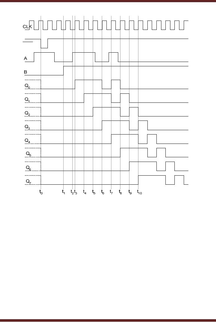
CLR
Figure
34.6b Timing diagram of a
74HC164, 8-bit Serial
In/Parallel Out Shift
Register
In the
timing diagram, the register
is cleared asynchronously by activating
the active-
low
CLR input at interval t0. The serial data is
applied at input A of the
register before
interval
t0. However, the register is
enabled to perform shift
operation at interval t1, when input B is
set
to logic
high. At interval t2,
there is a low to high
transition in the serial
data input which is
latch
by the
first flip-flop at the
positive clock transition at
interval t3. AT
each positive clock
transition
from
interval t4
to t10 the data is shifted
right by 1-bit.
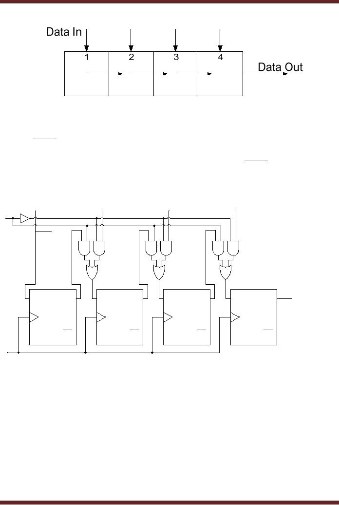
4. Parallel
In/Serial Out
Operation
The
register has parallel
inputs, data bits are
loaded into the register in
parallel by
activating a
load signal. The data is
shifted out serially by
application of clock signals.
Thus in
a 4-bit
shift register, after 4
clock signals the 4-bit
data is completely shifted
out of the shift
register.
Figure 34.7
350
CS302 -
Digital Logic & Design
Figure
34.7
Parallel
In/Serial Out
Operation
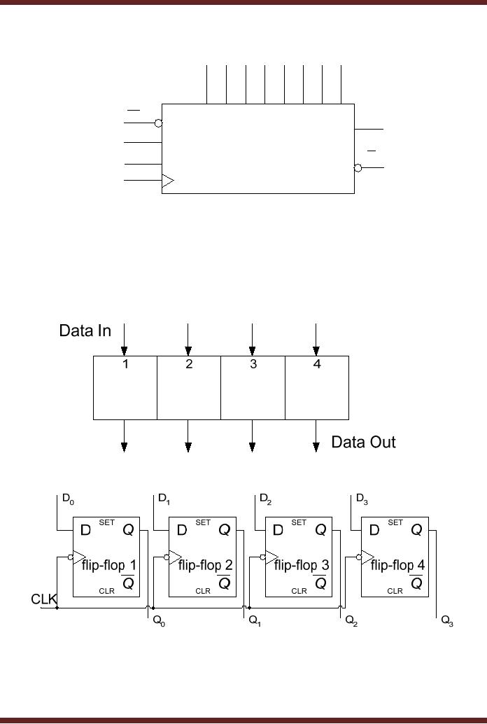
The
internal circuit of a 4-bit
Parallel In/Serial Out Shift
register is shown. Figure
34.8.
The
4-bit data is initially
loaded in Parallel into the
shift register by setting
the
SHIFT /
LOAD input to logic low.
The AND gates marked 2 are
enabled allowing data to
be
applied at
the inputs of the respective
D flip-flops. On a positive clock
transition the data
is
latched by
the respective flip-flops. To
shift the data, the
SHIFT /
LOAD is
set to logic high
which
enables AND gates marked 1
connecting the Q outputs of
the each flip-flop
connected
to the D
input of the next
flip-flop.
D0
D1
D2
D3
SHIFT /
LOAD
1
2
1
2
1
2
Q3
SET
SET
SET
SET
D
D
D
D
Q
Q
Q
Q
Q0
Q1
Q2
Serial
Data
flip-flop
1
flip-flop
2
flip-flop
3
flip-flop
4
Out
Q
Q
Q
Q
CLR
CLR
CLR
CLR
CLK
Figure
34.8
4-bit
Parallel In/Serial Out Shift
register
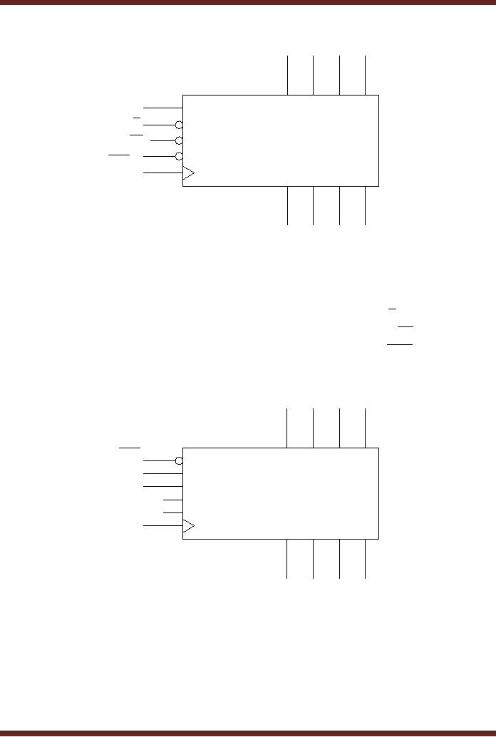
The
74HC165 is an 8-bit Parallel
In/Serial Out register which
can also work as an
8-bit
Serial
In/Serial Out register. The
Parallel Data is loaded
asynchronously by using
the
Asynchronous
Set/Clear Inputs. After
loading the parallel 8-bti
data, the serial shift
operation is
carried
out by enabling the clock
signal. The CLK and
CLK INH signal are
internally connected
through an OR
gate to the clock inputs of
the eight flip-flops. The
clock signal is enabled
by
setting
the CLK INH signal to logic
low. Figure 34.9.
351
CS302 -
Digital Logic & Design
D0 D1 D2 D3 D4 D5 D6 D7
SH / LD
Q7
SER
74HC165
CLK
INH
Q7
CLK
Figure
34.9
74HC165,
8-bit Parallel In/Serial Out
Shift Register
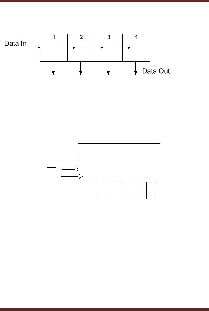
5. Parallel
In/Parallel Out
Operation
The
register has parallel inputs
and parallel outputs. Data
is entered in parallel by
applying a
single clock pulse. Data is
latched by the flip-flops on
the clock transition and
is
available in
parallel form at the
flip-flop outputs. Figure
34.10. The internal circuit
of 4-bit
Parallel
In/Parallel Out Register is
shown. Figure 34.11. The
Parallel In/Parallel Out
register
stores
Parallel data and usually
does not allows any
shift operations.
Figure
34.10 Parallel In/Parallel
Out Operation
Figure
34.11 A D-flip-flop based
4-bit Parallel In/Parallel
Out Register
352
CS302 -
Digital Logic & Design
D0 D1 D2 D3
J
K
74HC195
SH / LD
CLR
CLK
Q0 Q1 Q2 Q3
Figure
34.12 74HC195, 4-bit
Parallel In/Parallel Out
Shift Register
The
74HC195 is a 4-bit Parallel
In/Parallel Out Register. It
also has a Serial In
input,
therefore
the register can also be
used as a Serial In/Parallel
Out or as a Serial In/
Serial Out
register.
The output Q3 is
used as a Serial Out pin.
74HC195. The J and K inputs are used
to
input
data serially. These inputs
are connected to the first
flip-flop. The SH / LD is
used to load
the
Parallel Data and to allow
shift operations on the
clock transition. The CLR input is used
to
clear
the register asynchronously.
Figure 34.12.
D0 D1 D2 D3
CLR
S0
S1
74HC194
SR
SER
SL
SER
CLK
Q0 Q1 Q2 Q3
Figure
34.13 Bi-directional 4-bit
Universal Shift
Register
The
74HC194 is a 4-bit Bidirectional
Shift register that shifts
data in the left and
right
hand
directions and has both
Parallel and Serial input
and output capability.
Figure 34.13. The
register
has 4-bit Parallel Inputs
D0 to D3 and
Parallel Outputs Q0 to Q3. An active low
Asynchronous
CLR input clears the
register. The register
shifts data on a positive
clock
transition.
S0 and S1 inputs control the
operation of the register.
When S0
and S1 both are at
logic
high, the register loads
parallel data applied at the
inputs D0
to D3 on the clock
transition.
353
CS302 -
Digital Logic & Design
When
S0 is high, shift
right operation is carried
out, serial data is entered
through the SR SER
input.
When S1 is high, shift
left operation is carried
out, serial data is entered
through the SL
SER
input. When both S0 and S1
are
logic low the register is
inhibited.
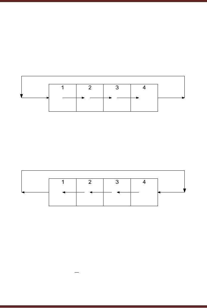
6. Rotate
Right Operation
The
serial output of the
register is connected to the
serial input of the
register. By
applying
clock pulses data is shifted
right. The data shifted
out of the serial out
pin at the right
hand
side is re-circulated back
into the shift register
input at the left hand
side. Thus the
data
is rotated
right within the register.
Figure 34.14
Figure
34.14 Rotate Right
Operation
7. Rotate
Left Operation
The
serial output of the
register is connected to the
serial input of the
register. By
applying
clock pulses data is shifted
left. The data shifted
out of the serial out
pin at the left
hand
side is re-circulated back
into the shift register
input at the right hand
side. Thus the
data
is rotated
left within the register.
Figure 34.15
Figure
34.15 Rotate Left
Operation
Shift
Register Counters
Shift
register counters are
basically, shift registers
connected to perform rotate
left and
rotate
right operations. When data
is rotated through a register
counter a specific sequence
of
states is
repeated. Two commonly used
register counters in digital
logic are the
Johnson
Counter
and the Ring
Counter.
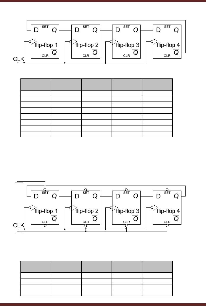
1. Johnson
Counter
In a Johnson
counter, the Q output of the last
flip-flop of the shift
register is connected
to the
data input of the first
flip-flop. The circuit of a
4-bit, D flip-flop based
Johnson Counter is
shown in
figure 34.16. The sequence
of states that are
implemented by a n-bit
Johnson
counter
are 2n. Thus a 4-bit
Johnson counter sequences
through 8 states and a 5-bit
Johnson
counter
sequences through 10 states.
Table 34.1
354
CS302 -
Digital Logic & Design
Figure
34.16 4-bit Johnson
Counter
Clock
Q0
Q1
Q2
Q3
Pulse
0
0
0
0
0
1
1
0
0
0
2
1
1
0
0
3
1
1
1
0
4
1
1
1
1
5
0
1
1
1
6
0
0
1
1
7
0
0
0
1
Table
34.1 Sequence of states of a
4-bit Johnson Counter
2. Ring
Counter
The
Ring Counter is similar to
the Johnson counter, except
that the Q output of the
last
flip-flop of
the shift register is
connected to the data input
of the first flip-flop of
the shift
register.
All the flip-flops of the
counter are cleared to logic
low except for the
first flip-flop
which is
preset to logic high. Figure
34.17.
PRE
CLR
Figure
34.17 4-bit Ring
Counter
After
the initialization of the
counter, the logic high
set at the output of the
first flip-flop
is shifted
right at each clock
transition. Table 34.2. With
a Ring Counter circuit no
decoding
gates
are required. Each state of
the ring counter has a
unique output.
Clock
Q0
Q1
Q2
Q3
Pulse
0
1
0
0
0
1
0
1
0
0
2
0
0
1
0
3
0
0
0
1
Table
34.2 Sequence of states of a
4-bit Ring Counter
355
Table of Contents:
- AN OVERVIEW & NUMBER SYSTEMS
- Binary to Decimal to Binary conversion, Binary Arithmetic, 1’s & 2’s complement
- Range of Numbers and Overflow, Floating-Point, Hexadecimal Numbers
- Octal Numbers, Octal to Binary Decimal to Octal Conversion
- LOGIC GATES: AND Gate, OR Gate, NOT Gate, NAND Gate
- AND OR NAND XOR XNOR Gate Implementation and Applications
- DC Supply Voltage, TTL Logic Levels, Noise Margin, Power Dissipation
- Boolean Addition, Multiplication, Commutative Law, Associative Law, Distributive Law, Demorgan’s Theorems
- Simplification of Boolean Expression, Standard POS form, Minterms and Maxterms
- KARNAUGH MAP, Mapping a non-standard SOP Expression
- Converting between POS and SOP using the K-map
- COMPARATOR: Quine-McCluskey Simplification Method
- ODD-PRIME NUMBER DETECTOR, Combinational Circuit Implementation
- IMPLEMENTATION OF AN ODD-PARITY GENERATOR CIRCUIT
- BCD ADDER: 2-digit BCD Adder, A 4-bit Adder Subtracter Unit
- 16-BIT ALU, MSI 4-bit Comparator, Decoders
- BCD to 7-Segment Decoder, Decimal-to-BCD Encoder
- 2-INPUT 4-BIT MULTIPLEXER, 8, 16-Input Multiplexer, Logic Function Generator
- Applications of Demultiplexer, PROM, PLA, PAL, GAL
- OLMC Combinational Mode, Tri-State Buffers, The GAL16V8, Introduction to ABEL
- OLMC for GAL16V8, Tri-state Buffer and OLMC output pin
- Implementation of Quad MUX, Latches and Flip-Flops
- APPLICATION OF S-R LATCH, Edge-Triggered D Flip-Flop, J-K Flip-flop
- Data Storage using D-flip-flop, Synchronizing Asynchronous inputs using D flip-flop
- Dual Positive-Edge triggered D flip-flop, J-K flip-flop, Master-Slave Flip-Flops
- THE 555 TIMER: Race Conditions, Asynchronous, Ripple Counters
- Down Counter with truncated sequence, 4-bit Synchronous Decade Counter
- Mod-n Synchronous Counter, Cascading Counters, Up-Down Counter
- Integrated Circuit Up Down Decade Counter Design and Applications
- DIGITAL CLOCK: Clocked Synchronous State Machines
- NEXT-STATE TABLE: Flip-flop Transition Table, Karnaugh Maps
- D FLIP-FLOP BASED IMPLEMENTATION
- Moore Machine State Diagram, Mealy Machine State Diagram, Karnaugh Maps
- SHIFT REGISTERS: Serial In/Shift Left,Right/Serial Out Operation
- APPLICATIONS OF SHIFT REGISTERS: Serial-to-Parallel Converter
- Elevator Control System: Elevator State Diagram, State Table, Input and Output Signals, Input Latches
- Traffic Signal Control System: Switching of Traffic Lights, Inputs and Outputs, State Machine
- Traffic Signal Control System: EQUATION DEFINITION
- Memory Organization, Capacity, Density, Signals and Basic Operations, Read, Write, Address, data Signals
- Memory Read, Write Cycle, Synchronous Burst SRAM, Dynamic RAM
- Burst, Distributed Refresh, Types of DRAMs, ROM Read-Only Memory, Mask ROM
- First In-First Out (FIFO) Memory
- LAST IN-FIRST OUT (LIFO) MEMORY
- THE LOGIC BLOCK: Analogue to Digital Conversion, Logic Element, Look-Up Table
- SUCCESSIVE –APPROXIMATION ANALOGUE TO DIGITAL CONVERTER