 |

Advanced Computer
Architecture-CS501
________________________________________________________
Advanced
Computer Architecture
Lecture
No. 25
Reading
Material
Handouts
Slides
Summary
�
Designing
a Parallel Input Port
�
Memory
Mapped I/O Ports
�
Partial
Decoding and the "wrap
around" Effect
�
Data Bus
Multiplexing
�
A generic
I/O Interface
�
The
Centronics Parallel Printer
Interface
Designing
a parallel input
port
The
following example illustrates a
number of important concepts.
Example
# 1
Problem
statement:
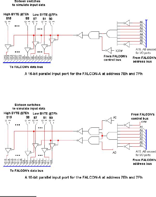
Design an
16-bit parallel input port
mapped on address 7Eh of the
I/O space of the
FALCON-A
CPU.
Solution:
The
process of designing a parallel
input port is very similar
to the design of a parallel
output
port except for the
following differences:
1. The
address in this case is 7Eh,
which is different from the
previous value.
Hence,
the address decoder will
have the inputs A7 and A0
inverted, while the
other
address lines at its input
will not be inverted.
2.
Control bus signal IOR# will be
used instead of the signal
IOW#.
3. A set
of sixteen tri-state buffers will be
used for data isolation.
Their common
enable
line will be connected to the
output of the big AND gate
(in the figure, fD
is being
inverted because Enable is
active low). The input of
these buffers can be
connected
to the input device and the
output is connected to the
FALCON-A's
data
bus.
In this
example, switches S15...S0 are
used to simulate the input
data. The complete
logic
circuit
is shown in the next two
figures.
Page
254
Last
Modified: 01-Nov-06
Advanced Computer
Architecture-CS501
________________________________________________________
In the
second figure, the CPU is
assumed to allow the use of
some part of its data
bus
during a
transfer, while in the first
figure it is not
allowed.
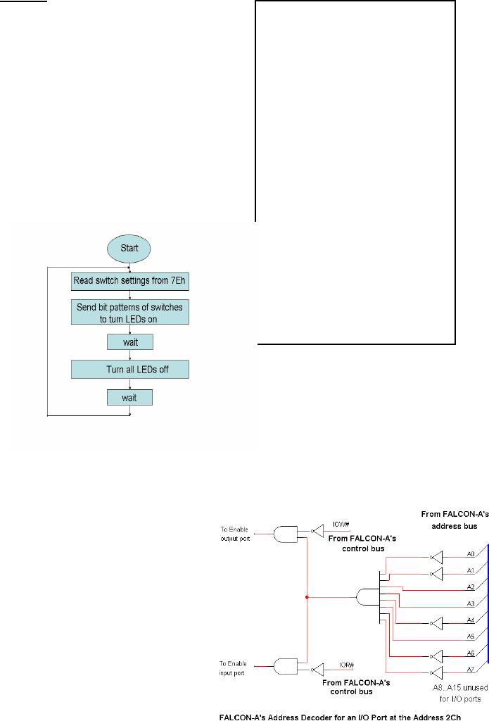
Example
# 2
Problem
statement:
Given a
FALCON-A processor with a
16-bit parallel input port
at address 7Eh and a
16-
bit
parallel output port at
address DEh. Sixteen LED
branches are used to display
the
data at
the output port and sixteen
switches are used to send
data through the input
port.
Write an
assembly language program to
continuously monitor the
input port and blink
the
LED or
LED(s) corresponding to the
switch (es) set to logic 1.
For example, if S0 and S2
are
set to 1, then only the
LEDs L0 and L2 should blink. If S7 is
also set to logic 1
later,
then L7
should also start
blinking.
Page
255
Last
Modified: 01-Nov-06
Advanced Computer
Architecture-CS501
________________________________________________________
Solution:
The
program is shown in the text
box with
;filename:
Example_2.asmfa
filename:
Example_2. It works as
explained
;Notes:
below:
;
r1 is
used as an I/O register
The
first two instructions read
the input port at
;
r2 is
used as a delay
counter
address
7Eh and send this bit
pattern to the
;
output
port at address DEh. This
will cause the
start:
in r1, 126
; 126d =
7Eh
LEDs
corresponding to the switches
that are set
out
r1, 222
; 222d =
DEh
to a 1 to
turn on. Next, the
program waits for a
;
suitable
amount of time, and then
turns all
movi
r2, 0
LEDs
off and waits again.
delay1:
subi r2, r2, 1
After
the second wait, the
program reads the
jnz
r2, [delay1]
input
port again. The LEDs
that will be turn on
;
at the
output port will now be
according to the
movi
r1, 0
; all
LEDs off
new
switch settings at the input
port. The
out
r1, 222
process
repeats indefinitely. Please
see the
;
movi
r2, 0
delay2:
subi r2, r2, 1
jnz
r2, [delay2]
;
jump
[start]
;
halt
flowchart
also.
It is also possible to
use a single
address
for both the input and
the
output
port. The following
diagram
shows an
address decoder for a
16-
bit
parallel input/output port
at
address
2Ch of the FALCON-A's
I/O
space. Note that the
control bus lines IOW# and
IOR# will differentiate between
the
register
and the tri-state
buffer.
Page
256
Last
Modified: 01-Nov-06
Advanced Computer
Architecture-CS501
________________________________________________________
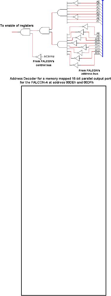
Memory
mapped I/O ports
If it is
desired to map the
16-bit
output
port of Example
#1(lec24)
on the
memory space of the
FALCON-A,
the
following
changes
would be needed.
1. Replace
the IOW# signal
with
the MEMW# signal.
2. Use
the entire CPU
address
bus at
the input of the
address
decoder, as shown
in the
next figure. This
address
decoder uses the
;filename:
Example_2MM.asmfa
addresses
00DEh and 00DFh of
the
;Notes:
FALCON-A's
memory space.
;
For
MEMORY MAPPED
3. Use
the store
instruction
instead of the
;
output
port at 00DEh
out
instruction
for sending data to
the
;
output
port (for memory mapped
input
;
r6 holds
the output address
ports,
use the load
instruction
instead of
;
r7 holds
the input address
the
in
instruction).
;
The
program for Example
#2(lec25) is rewritten
movi
r6, 111
for
the case of a memory mapped
output port,
add
r6, r6, r6
and is
shown in the attached text
box. The
;
advantage will be
that more than 256 ports
are
movi
r7, 126
available,
but the disadvantage is that
the
;
address
decoder will become more
complex,
;
r1 is
used as an I/O register
resulting
in increased hardware costs.
;
r2 is
used as a delay
counter
To avoid
the increase in hardware
complexity,
;
many
architects use what is
called "partial
start:
load
r1,[r7] ; 126d =
7Eh
decoding".
This is explained in the
next section.
store
r1, [r6] ; 222d =
DEh
;
Partial
decoding
and
the
"wrap
movi
r2, 0
around"
effect
delay1:
subi r2, r2, 1
jnz
r2, [delay1]
Partial
decoding is a technique in which
some
;
of the
CPU's address lines forming
an input to
movi
r1, 0
; all
LEDs off
the
address decoder are ignored.
This reduces
store
r1, [r6]
the
complexity of the address decoder, and
also
;
lowers
the cost. As an example, if
the address
movi
r2, 0
lines
A8...A15 from the FALCON-A
are not
delay2:
subi r2, r2, 1
used in
the address decoder of the
previous
jnz
r2, [delay2]
figure,
this will save eight
inverters and two
;
AND
gates. Partial decoding is an
attractive
jump
[start]
choice in
small systems, where the size of
the
;
halt
Page
257
Last
Modified: 01-Nov-06
Advanced Computer
Architecture-CS501
________________________________________________________
address
space is large but most of
the memory is unimplemented.
However, partial
decoding
has its price as well.
Consider the memory map for
the
FALCON-A,
shown again in the next
figure. With 16 address
lines, the total
address
space is
216 = 64 Kbytes. When
the
upper
eight address lines are
unused,
they
become don't cares. The
port
shown in
the previous figure will
be
accessed
for address 00DEh. But,
it
will also be
accessed for address
01DEh,
02DEh,......, FFDEh. In
fact,
the 64
Kbyte address space has
been
reduced to a 256
byte space. It
"wrapped
around" itself 256 times.
If
we only
left 6 address lines, i.e.,
A15
...
A10, unconnected, then we will
still
have a
"wrap around", but of
a
different
type. Now a 1 Kbyte (= 210 )
address
area will wrap around itself
64 times (= 26
).
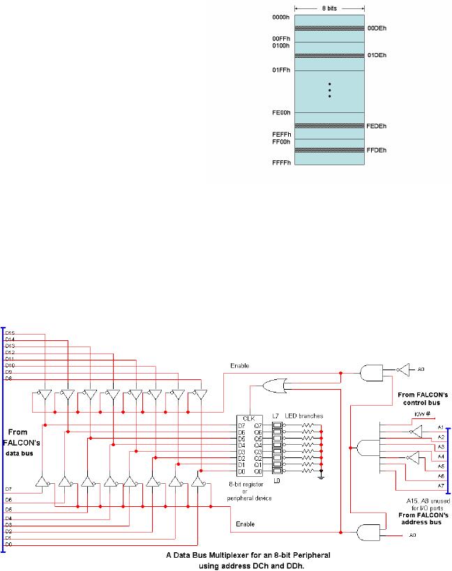
Data
bus multiplexing
Data bus
multiplexing refers to the
situation when one part of
the data bus is connected
to
the
peripheral's data bus at one time and
the second part of the
data bus is connected to
the
peripheral's data bus at a different
time in such a way that at
one time, only one
8-bit
portion
of the data bus is connected to
the peripheral.
Page
258
Last
Modified: 01-Nov-06
Advanced Computer
Architecture-CS501
________________________________________________________
Consider
the situation where an 8-bit
peripheral is to be interfaced with a
CPU that has a
16-bit
(or larger) data bus,
but a byte-wide address
space. Each byte transferred
over the
data bus
will have a separate address
associated with it. For
such CPUs, data bus
multiplexing
can be used to attach 8-bit
peripherals requiring a block of
addresses. Tri-
state
buffers can be used for
this
purpose as
shown in the attached figure.
The logic circuit shown is
for an 8-bit parallel
output
port using addresses DCh and
DDh of the FALCON's I/O
address space. It is
assumed
that the CPU allows
the use of a part of its
data bus during a transfer, and
that
each
16-bit general purpose register can be
used as two separate 8-bit
registers, e.g., r1
can be
split as r1L and r1H such
that
r1L<7..0>
:= r1<7..0>, and
r1H<7..0>
:= r1<15..8>
The
LED branches and the 8-bit
register shown in the
diagram serve as a place holder,
and can be replaced by
a peripheral device in actual
practice. For an even
address, A0=0,
and the
upper group of the tri-state
buffers is enabled, thereby connecting
D<15..8> of
the
CPU to the peripheral, while
for an odd address from the
CPU, A0=1, and the
lower
group of
the tri-state buffers is enabled.
This causes D<7..0> of
the CPU to be
connected
with
the peripheral device. In
such systems the instruction
out
r1H,220 will
access the
peripheral
device using D<15..8>,
while the instruction out
r1L,221 will
access it using
D<7..0>.
The instruction out
r1,220 will send
r1H to the peripheral and
the contents of
r1L will
be lost. Why? This is left
as an exercise for the student.
The advantage of data
bus
multiplexing is that all
addresses are utilized and
none of them is wasted, while
the
disadvantage is
the increased complexity and cost of
the interface.
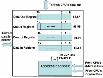
A
generic I/O interface
Most
parallel I/O ports used
with
peripheral
devices are mapped on a
range of
contiguous addresses.
The
following
figure shows the
block
diagram
of part of an interface that
can
be used
with a typical parallel
printer.
It used
eight consecutives
addresses:
address
56 to 63. A similar
interface
can be
used with the FALCON-A.
The
registers
shown within the interface
are
associated
with some parallel device,
and have some pre-defined
functions. For
example,
the 16
bit register at addresses 56 and 57 can
be used as a "data out"
register for sending
data
bytes to the parallel
device. In the same way,
the register at addresses 60 and 61
can
be used
by the CPU to send control
bits to the device. The
double arrow shown at the
top
corresponds to
the data bus connection of
the interface with the
CPU. The address
decoder
shown at the bottom receives
address and control information
from the CPU and
generates
enable signals for these registers. These
abstract concepts are further
explained
in
Example #3(lec25).
Page
259
Last
Modified: 01-Nov-06

Advanced Computer
Architecture-CS501
________________________________________________________
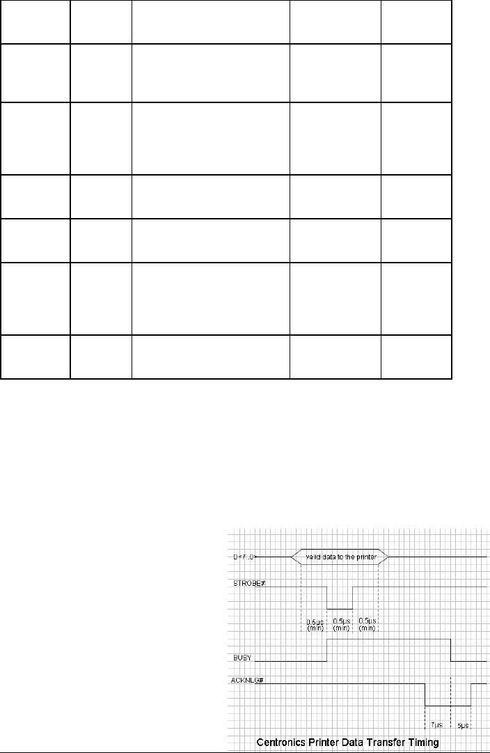
The
Centronics Parallel Printer
Interface
The
Centronics Parallel Printer
Interface is an example of a real,
industry standard, set of
signal
specifications used by most
printer manufacturers. It was originally
developed for
Centronics
printers and can be used by devices
having a uni-directional,
byte-wide
parallel
interface. Table 1 shows the
important signals and their
functions as defined by
the
Centronics standard. Note that
the direction of the signals
is with respect to the
printer
and not
with respect to the
CPU.
Typically,
the printer (or any
other similar device) is
connected to the CPU via a
cable
which
has a 25-pin connector at
the CPU side and a 36-pin
connector at the printer
side.
Every
data bit in the 8-bit
data bus D<7...0> uses a
twisted pair for
suppressing
transmission-line
effects, like radiation and noise.
The return path of these
pins should
always be
connected to signal ground.
Additionally, the entire
printer cable should be
shielded,
and connected to chassis ground on
each side. The three
signals STROBE#,
BUSY and
ACKNLG# form a set of
handshaking signals. By using
these signals, the
CPU can
communicate asynchronously with
the printer, as shown in the
accompanying
timing
waveforms. When the printer
is ready for printing, the
CPU starts data transfer
to
the
printer by placing the 8-bit
data (corresponding to the
ASCII value of the character
to
be
printed) on the printer's
data bus (pin 2 through 9 on
the 36-pin connector, as
shown in
Table
1). After this, a negative
pulse of duration at least 0.5�s is
applied to the
STROBE#
input
(pin1) of the printer. The
minimum set-up and hold
times of the latches within
the
printer
are specified as 0.5�s each, and
these timing requirements
must be observed by
the
CPU (the interface designer
should make sure that these
specifications are met).
As
soon as
STROBE# goes low, the
printer activates its BUSY
line (pin 11) which is
an
indication
to the CPU that additional
bytes cannot be accepted.
The CPU can monitor
this
status
signal over an input port (a
detailed assignment of these signals to
I/O port bits is
given in
Table 2).
Table
1: The Centronics Parallel Printer
Interface
(power
and ground signals are not
shown)
Pin#
Pin#
(36-DB)
Function
(25-DB)
Signal
Direction
Printer
Summary
CPU
Name
w.r.t.
side
side
Printer
D<7..0>
Input
8-bit
data bus
9,8,...,2
9,8,...,2
1-bit
control signal
STROBE#
Input
High:
default value.
1
1
Low:
read-in of data is
performed.
1-bit
status signal
Low:
data has been
received
ACKNLG#
Output
and the
printer is ready to
10
10
accept
new data.
High:
default value.
Page
260
Last
Modified: 01-Nov-06
Advanced Computer
Architecture-CS501
________________________________________________________
1-bit
status signal
BUSY
Output
Low:
default value
11
11
High:
see note#1
1-bit
status signal
PE#
Output
High:
the printer is out of
12
12
paper.
Low:
default value.
1-bit
control signal
INIT#
Input
Low:
the printer controller
is
16
31
reset to
its initial state and
the
print buffer is cleared.
High:
default value.
1-bit
status signal
SLCT
Output
High:
the printer is in
13
13
selected
state.
1-bit
control signal
AUTO
Input
Low:
paper is automatically
14
14
FEED
XT#
fed
after one line.
1-bit
control signal
Low:
data entry to the
SLCT
IN#
Input
printer
is possible.
17
36
High:
data entry to printer
is
not
Possible.
1-bit
status signal
ERROR#
Output
Low:
see note#2.
15
32
High:
default value.
Note#1
The
printer can not read data
due to one of the following
reasons:
1) During
data entry
2) During
data printing
3) In
offline state
4) During
printer error status
Note#2
When
the printer is in one of the
following states:
1) Paper
end state
2)
Offline state
3) Error
state
When
this character is
completely
received,
the ACKNLG# signal (pin
10)
goes
low, indicating that the
transfer is
complete.
Soon after this, the BUSY
signal
returns
to logic zero, indicating
that a new
transfer
can be initiated. The BUSY
signal
is
more suitable for
level-triggered
Page
261
Last
Modified: 01-Nov-06
Advanced Computer
Architecture-CS501
________________________________________________________
systems,
while the ACKNLG# signal is
better for edge-triggered systems.
The
interface will typically use
two eight bit parallel
output ports of the CPU, one
for the
ASCII
value of the character byte
and the other for the
control byte. It also specifies an
8-
bit
parallel input port for
the printer's status information
that can be checked by the
CPU.
Table
2: Centronics Bit Assignment For I/O
Ports
Logic
Descript
7
6
5
4
3
2
1
0
al
ion
Addre
ss
0
8-bit
D<7>
D<6>
D<5
D<4>
D<3>
D<2>
D<1>
D<0>
output
>
port
for
DATA
1
8-bit
BUS
ACKNL
PE#
SLC
ERRO
Unus
Unus
Unused
input
Y
G#
T
R#
ed
ed
port
for
STATUS
2
8-bit
Unus
Unused
DIR
IRQE
SLCT
INIT
Auto
STROB
15
output
ed
N
IN#
#
Feed
E#
port
for
XT#
CONTR
OL
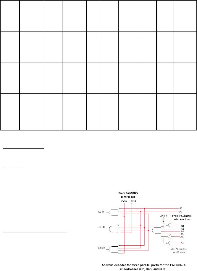
Example
# 3:
Problem
statement:
Design a
Centronics parallel printer
interface for the FALCON-A
CPU. Map
this
interface
starting at address 38h (56
decimal) of the FALCON-A's I/O
address space.
Solution:
The
Centronics interface requires at least
three I/O addresses. However,
since
the
FALCON-A
has a 16-bit data bus, and
since we do not want to implement
data
bus
multiplexing
(to keep things simple), we
will use three contiguous
even addresses,
i.e.,
38h,
3Ah and 3Ch for the
address
decoder
design. This arrangement also
conforms
to the requirements of
our
assembler.
Moreover, we will connect
data
bus lines D7...D0 of
the
FALCON-A
to the 8-bit data bus
of
15
This bit,
when set, enables the
bidirectional mode.
Page
262
Last
Modified: 01-Nov-06
Advanced Computer
Architecture-CS501
________________________________________________________
the
printer (i.e. pins 9, 8, ...
, 2 of the printer cable) and
leave lines D15...D8
unconnected.
Since the
FALCON-A uses the big-endian
format, this will make sure that
the low byte of
CPU
registers will be transferred to the
printer. (Recall that these
bytes will actually be
mapped on
addresses 39h, 3Bh and 3Dh).
The logic diagram of the
address decoder for
this
interface is shown in the
given figure.
Page
263
Last
Modified: 01-Nov-06
Table of Contents:
- Computer Architecture, Organization and Design
- Foundations of Computer Architecture, RISC and CISC
- Measures of Performance SRC Features and Instruction Formats
- ISA, Instruction Formats, Coding and Hand Assembly
- Reverse Assembly, SRC in the form of RTL
- RTL to Describe the SRC, Register Transfer using Digital Logic Circuits
- Thinking Process for ISA Design
- Introduction to the ISA of the FALCON-A and Examples
- Behavioral Register Transfer Language for FALCON-A, The EAGLE
- The FALCON-E, Instruction Set Architecture Comparison
- CISC microprocessor:The Motorola MC68000, RISC Architecture:The SPARC
- Design Process, Uni-Bus implementation for the SRC, Structural RTL for the SRC instructions
- Structural RTL Description of the SRC and FALCON-A
- External FALCON-A CPU Interface
- Logic Design for the Uni-bus SRC, Control Signals Generation in SRC
- Control Unit, 2-Bus Implementation of the SRC Data Path
- 3-bus implementation for the SRC, Machine Exceptions, Reset
- SRC Exception Processing Mechanism, Pipelining, Pipeline Design
- Adapting SRC instructions for Pipelined, Control Signals
- SRC, RTL, Data Dependence Distance, Forwarding, Compiler Solution to Hazards
- Data Forwarding Hardware, Superscalar, VLIW Architecture
- Microprogramming, General Microcoded Controller, Horizontal and Vertical Schemes
- I/O Subsystems, Components, Memory Mapped vs Isolated, Serial and Parallel Transfers
- Designing Parallel Input Output Ports, SAD, NUXI, Address Decoder , Delay Interval
- Designing a Parallel Input Port, Memory Mapped Input Output Ports, wrap around, Data Bus Multiplexing
- Programmed Input Output for FALCON-A and SRC
- Programmed Input Output Driver for SRC, Input Output
- Comparison of Interrupt driven Input Output and Polling
- Preparing source files for FALSIM, FALCON-A assembly language techniques
- Nested Interrupts, Interrupt Mask, DMA
- Direct Memory Access - DMA
- Semiconductor Memory vs Hard Disk, Mechanical Delays and Flash Memory
- Hard Drive Technologies
- Arithmetic Logic Shift Unit - ALSU, Radix Conversion, Fixed Point Numbers
- Overflow, Implementations of the adder, Unsigned and Signed Multiplication
- NxN Crossbar Design for Barrel Rotator, IEEE Floating-Point, Addition, Subtraction, Multiplication, Division
- CPU to Memory Interface, Static RAM, One two Dimensional Memory Cells, Matrix and Tree Decoders
- Memory Modules, Read Only Memory, ROM, Cache
- Cache Organization and Functions, Cache Controller Logic, Cache Strategies
- Virtual Memory Organization
- DRAM, Pipelining, Pre-charging and Parallelism, Hit Rate and Miss Rate, Access Time, Cache
- Performance of I/O Subsystems, Server Utilization, Asynchronous I/O and operating system
- Difference between distributed computing and computer networks
- Physical Media, Shared Medium, Switched Medium, Network Topologies, Seven-layer OSI Model