 |

Advanced Computer
Architecture-CS501
________________________________________________________
Advanced
Computer Architecture
Lecture
No. 23
Reading
Material
Vincent
P. Heuring & Harry F. Jordan
Chapter
8
Computer
Systems Design and Architecture
8.1,
8.2
Summary
·
Introduction
to I/O Subsystems
·
Major
Components of an I/O Subsystems
·
Computer
Interface
·
Memory
Mapped I/O versus Isolated
I/O
·
Considerations
during I/O Subsystem
Design
·
Serial
and Parallel Transfers
·
I/O
Buses
Introduction
to I/O Subsystems
This
module is about the
computer's input and output. As we
have seen in the case
of
memory
subsystems, that when we use
the terms " read" and
"write", then these
terms
are
from the CPU's point of
view. Similarly, when we use
the terms "input" and
"output"
then
these are also from the
CPU's point of view. It
means that when we are
talking about
an input
cycle, then the CPU is
receiving data from a
peripheral device and the
peripheral
device is
providing data. Similarly,
when we talk about an output
cycle then the CPU
is
sending
data to a peripheral device and
the peripheral device is
receiving data. I/O
Subsystems
are similar to memory subsystems in
many aspects. For example,
both
exchange
bits or bytes. This transfer
is usually controlled by the
CPU. The CPU
sends
address
information to the memory and
the I/O subsystems. Then these
subsystems
decode
the address and decide which
device should be involved in
the transfer. Finally
the
appropriate data is exchanged between
the CPU and the memory or
the I/O device.
Memory
and I/O subsystems differ in the
following ways:
1. Wider
range of data transfer
speed:
I/O devices can be
very slow such as a keyboard
in which case the interval
between
two
successive bytes (or
keystrokes) can be in seconds. On the
other extreme, I/O
devices can be
very fast such as a disk
drive sending data to the
CPU or a stream of
packets
arriving over a network, in
which case the interval
between two
successive
bytes can
be in microseconds or even nanoseconds. While I/O
devices can have such
a wide
range of data transfer speed compared to
the CPU's speed, the
case of memory
devices is
not so. Even if a memory
device is slow compared to the
CPU, the CPU's
speed can
be made compatible by inserting
wait states in the bus
cycle.
Page
234
Last
Modified: 01-Nov-06

Advanced Computer
Architecture-CS501
________________________________________________________
2.
Asynchronous activity:
Memory
subsystems are almost always
synchronous. This means that
most memory
transfers
are governed by the CPU's
clock. Generally this is not
the case with I/O
subsystems.
Additional signals, called
handshaking signals, are
needed to take care of
asynchronous
I/O transfers.
3. Larger
degradation in data quality:
Data
transferred by I/O subsystems can carry
more noise. As an example,
telephone
line
noise can become part of the
data transferred by a modem.
Errors caused by
media defects on
hard drives can corrupt the
data. This implies that
effective error
detection
and correction techniques must be
used with I/O subsystems.
4.
Mechanical nature of many I/O
devices:
Many I/O
devices or a large portion of I/O devices
use mechanical parts
which
inherently
have a high failure rate. In
case an I/O device fails,
interruptions in data
transfer
will occur, reducing the
throughput. As an example, if a printer
runs out of
paper,
then additional bytes cannot
be sent to it. The CPU's
data should be
buffered
(or
kept in a temporary place)
till the paper is supplied
to the printer, otherwise
the
CPU will
not be able to do anything else
during this time.
To deal
with these differences, special
software programs called
device drivers are
made
a part of
the operating system. In
most cases, device drivers
are written in
assembly
language.
You would
recall that in case of
memory subsystems, each location
uses a unique address
from
the CPU's address space.
This is generally not the
case with I/O devices. In
most
cases, a
group or block of contiguous
addresses is assigned to an I/O device,
and data is
exchanged
byte-by-byte. Internal buffers
(memory) within the device
store this data if
needed.
In the
past, people have paid a lot of
attention to improve the
CPU's performance, as a
result of
which the performance
improvement of I/O subsystems was ignored.
(I/O
subsystems
were even called the
"orphans" of computer architecture by
some people).
Perhaps,
many benchmark programs and
metrics that were developed
to evaluate
computer
systems focused on the CPU or
the memory performance only.
Performance of
I/O subsystems is as
important as that of the CPU
or the memory, especially in
today's
world.
For example, the transaction
processing systems used in airline
reservation
systems or
the automated teller
machines in banks have a very
heavy I/O traffic,
requiring
improved I/O performance. To illustrate
this point, look at the
following
example.
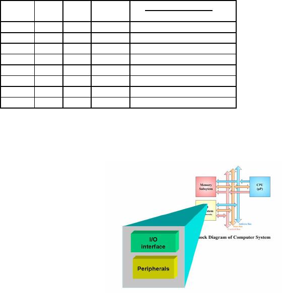
Suppose
that a certain program takes
200 seconds of elapsed time to
execute. Out of
these 200
seconds, 180 seconds is the
CPU time and the rest is I/O
time. If the CPU
performance
improves by 40% every year
for the next seven years
because of
developments
in technology, but the I/O
performance stays the same,
let us look at the
following
table, which shows the
situation at the end of each
year. Remember that
Elapsed
time = CPU time + I/O
time.
This
gives us the I/O time = 200 180 =
20 seconds at the beginning,
which is 10 % of
the
elapsed time.
Page
235
Last
Modified: 01-Nov-06
Advanced Computer
Architecture-CS501
________________________________________________________
Year
# CPU I/O Elapsed
I/O
Time x100 %
Elapsed
Time
Time
Time Time
0
180
20
200
10
%
1
129
20
149
13.42
%
2
92
20
112
17.85
%
3
66
20
86
23.25
%
4
47
20
67
29.85
%
5
34
20
54
37.03
%
6
24
20
44
45.45
%
7
17
20
37
54.05
%
It can be
easily seen that over seven
years, the I/O time will
become more than 50 %
of
the
total time under these
conditions. Therefore, the
improvement of I/O performance is
as
important as the improvement of
CPU performance. I/O performance will
also be
discussed
in detail in a later
section.
Major
components of an I/O
subsystem
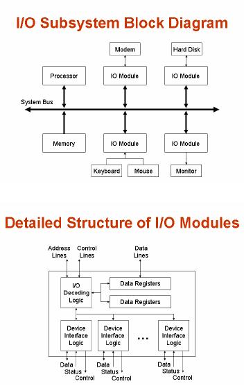
I/O subsystems
have two major
parts:
·
The I/O
interface, which is
the
electronic
circuitry that
connects
the
CPU to the I/O
device.
·
Peripherals,
which are
the
devices
used to communicate with
the
CPU,
for
example,
the
keyboard,
the monitor, etc.
Computer
Interface
A
Computer Interface is a piece of
hardware whose primary purpose is to
connect
together
any of the following types
of computer elements in such a
way that the
signal
levels
and the timing requirements of
the elements are matched by
the interface. Those
elements
are:
· The
processor unit
· The
memory subsystem(s)
· Peripheral
(or I/O) devices
· The
buses (also called
"links")
In other
words, an interface is an electronic
circuit that matches the
requirements of the
two
subsystems between which it is connected.
An interface that can be used to
connect
Page
236
Last
Modified: 01-Nov-06
Advanced Computer
Architecture-CS501
________________________________________________________
the
microcomputer bus to peripheral devices is
called an I/O Port. I/O ports serve
the
following
three purposes:
· Buffering
(i.e., holding temporarily)
the data to and from the
computer bus.
· Holding
control information that dictates
how a transfer is to be
conducted.
·
Holding
status information so that the
processor can monitor the
activity of the
interface
and its associated I/O
element.
This
control information is usually
provided by the CPU and is
used to tell the
device
how to
perform the transfer, e.g.,
if the CPU wants to tell a
printer to start a new
page,
one of
the control signals from
the CPU can be used for a
paper advance command,
thereby
telling the printer to start
printing from the top of
the next page. In the
same way
the
CPU may send a control
signal to a tape drive
connected in the system
asking it to
activate
the rewind mechanism so that
the start of the tape is
positioned for access by
the
CPU.
Status information from various devices
helps the CPU to know
what is going on in
the
system. Once again, using
the printer as an example, if
the printer runs out of
paper,
this
information should be sent to the
CPU immediately. In the same
way, if a hard drive
in the
system crashes, or if a sector is damaged
and cannot be read, this
information
should
also be conveyed to the CPU as soon as
possible
The
term "buffer" used in the
above discussion also needs to be
understood. In most
cases,
the word buffer refers to
I/O registers in an interface where data,
status or control
information
is temporarily stored. A block of memory
locations within the main
memory
or within
the peripheral devices is also called a
buffer if it is used for
temporary storage.
Special
circuits used in the
interfaces
for
voltage/current matching, at
the
input and
the output, are also
called
buffers.
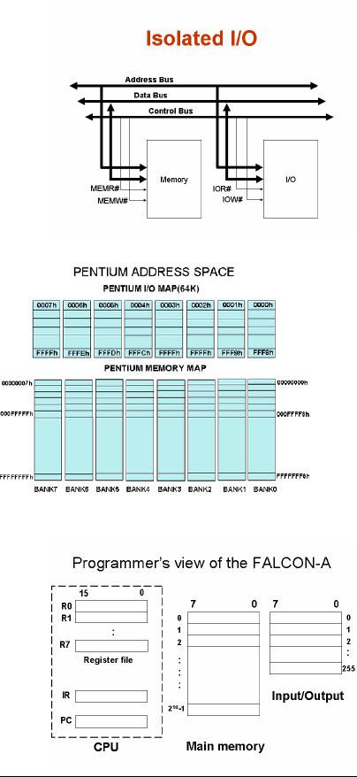
The
given figure shows a
block
diagram
of a typical I/O subsystem
connected
with the other
components
in a
computer. The thick
horizontal
line is
the system bus that serves
as a
back-bone
in the entire
computer
system.
It is used to connect
the
memory
subsystems as well as the I/O
subsystems
together. The CPU
also
connects
to this bus through a
"bus
interface
unit", which is not shown
in
this
figure. Four I/O modules
are
shown in
the figure. One module
is
used to
connect a keyboard and a
mouse to
the system bus. A
second
module
connects a monitor to
the
system
bus. Another module is
used
with a
hard disk and a fourth
I/O
module is
used by a modem. All
these
Page
237
Last
Modified: 01-Nov-06
Advanced Computer
Architecture-CS501
________________________________________________________
modules
are examples of I/O ports. A
somewhat detailed view of
these modules is
shown
in the
next figure.
As we
already know that the
system bus actually consists of three
buses, namely the
address
bus, the data bus and the
control bus. These three
buses are being applied to
the
I/O
module in this figure. At
the bottom, we see a set of
data, status and control
lines
from
each "device interface
logic" block. Each of these
sets connects to a
peripheral
device.
I/O decoding logic is also shown in
this figure.
Memory
Mapped I/O versus Isolated I/O
Although
this concept was explained
earlier as
well, it
will be useful to review it again in
this
context.
In isolated I/O, a separate
address
space of
the CPU is reserved for
I/O
operations.
This address space is
totally
different
from the address space
used for
memory
devices. In other words, a CPU
has
two
distinct address spaces, one
for memory
and one
for input/output. Unique
CPU
instructions
are associated with the I/O
space,
which
means that if those instructions
are
executing
on the CPU, then the
accessed
address
space will be the I/O space and
hence
the
devices mapped on the I/O
space.
The
x86 family with the
in
and
the out
instructions
is a well known
example
of
this situation. Using
the in
instruction,
the Pentium processor
can
receive
information from a
peripheral
device,
and using the out
instruction,
the
Pentium processor can
send
information
to a peripheral device.
Thus,
the I/O devices are mapped
on
the I/O
space in case of the
Pentium
processor. In
some processors, like
the
SRC,
there is no separate I/O space.
In
this
case, some address space
out of
the
memory address space must be
used to map I/O devices. The benefit will
be that all
the
instructions which access
memory can be used for I/O devices.
There is no need for
including
separate I/O instructions in the
ISA
of the
processor. However, the
disadvantage
will be
that the I/O interface will
become
complex.
If partial decoding is used to
reduce
the
complexity of the I/O interface,
then a lot
of memory
addresses will be consumed.
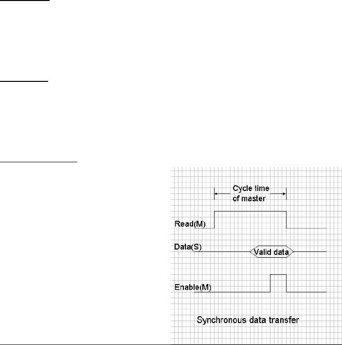
The
given
figure shows the memory
address space
Page
238
Last
Modified: 01-Nov-06
Advanced Computer
Architecture-CS501
________________________________________________________
as well
as the I/O address space for
the Pentium processor. The I/O
space is of size 64
Kbytes,
organized as eight banks of 8 Kbytes
each.
A similar
diagram for the FALCON-A was
shown earlier and is repeated here
for easy
reference.
The
next question to be answered is how
the CPU will differentiate
between these two
address
spaces. How will the system
components know whether a
particular transfer is
meant
for memory or an I/O device? The
answer is simple: by using
signals
from
the control bus, the
CPU will indicate which
address space is meant
during a
particular
transfer. Once again, using
the Pentium as an example, if
the in
instruction
is
executing
on the processor, the IOR#
signal will become active and
the MEMR# signal
will be
deactivated. For a mov
instruction,
the control logic will
activate the MEMR#
signal
instead of the IOR#
signal.
Considerations
during I/O Subsystem Design
Certain
things must be taken care of
during the design of an I/O
subsystem.
Data
location:
The
designer must identify the
device where the data to be
accessed is available,
the
address
of this device and how to
collect the data from
this device. For example, if
a
database
needs to be searched for a
record that is stored in the
fourth sector of the
second
track of
the third platter on a
certain hard drive in the
system, then this
information is
related
to data location. The
particular hard drive must
be selected out of the
possibly
many
hard drives in the system,
and the address of this
record in terms of platter
number,
track
number and sector number must be
given to this hard
drive.
Data
transfer:
This
includes the direction of
transfer of data; whether it is out of
the CPU or into
the
CPU,
whether the data is being
sent to the monitor or the
hard drive, or whether it
is
being
received from the keyboard
or the mouse. It also includes the
amount of data to be
transferred
and the rate at which it should be
transferred. If a single mouse click is
to be
transferred
to the CPU, then the
amount of data is just one
bit; on the other hand, a
block
of data
for the hard drive
may be several kilo bytes.
Similarly, the rate of the
transfer of
data to a
printer is very different
from the transfer rate
needed for a hard
drive.
Data
synchronization:
This
means that the CPU
should input data
from an
input device only when
the device is
ready to
provide data and send data
to an
output
device only when it is ready
to receive
data.
There
are three basic schemes
which can be
used
for synchronization of an I/O
data
transmission:
· Synchronous
transmission
· Semi-synchronous
transmission
· Asynchronous
transmission
Synchronous
transmission:
Page
239
Last
Modified: 01-Nov-06
Advanced Computer
Architecture-CS501
________________________________________________________
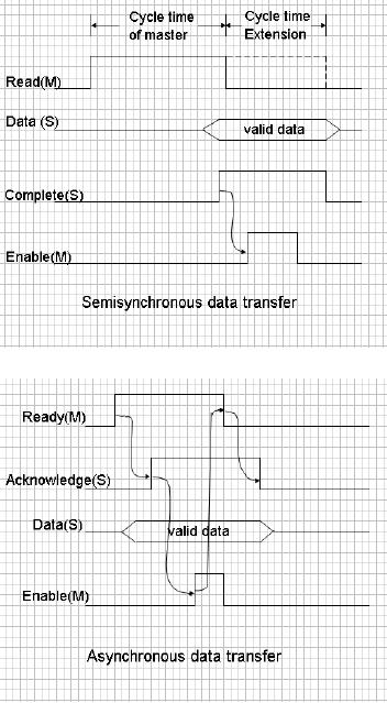
This can
be understood by looking at the
waveforms shown in Figure
A.
M stands
for the bus master and S stands
for the slave device on
the bus. The master
and
the
slave are assumed to be
permanently connected together, so
that there is no need
for
the
selection of the particular
slave device out of the
many devices that may be present
in
the
system. It is also assumed that
the slave device can perform
the transfer at the
speed
of the
master, so no handshaking signals are
needed.
At the
start of the transfer
operation, the master activates
the Read signal, which
indicates
to the
slave that it should respond
with data. The data is
provided by the slave, and
the
master
uses the Enable signal to
latch it. All
activity
takes place synchronously with
the
Figure
A
system
clock (not shown in the
figure). A
familiar
example of synchronous transfer is a
register-to-register transfer within a
CPU.
Semi-synchronous
transmission:
Figure B
explains this type of
transfer. All activity is still
synchronous with the
system
clock,
but in some situations, the
slave device
may
not be able to provide the
data to the
master
within the allotted time.
The additional
time
needed by the slave, can be
provided by
adding an
integral number of clock periods
to
Figure
A
the
master's cycle time.
The
slave indicates its
readiness by activating
the
complete signal. Upon
receiving this
signal,
the master activates the
Enable signal
to latch
the data provided by the
slave.
Transfers
between the CPU and the
main
memory
are examples of
semi-synchronous
transfer.
Asynchronous
transmission:
This
type of transfer does not
require a
common
clock. The master and the
slave
Figure
B
operate
at different speeds.
Handshaking
signals
are necessary in this case,
and are used
to
coordinate the data transfer
between the
master and
the slave as shown in the
Figure C.
When
the master wants to initiate a
data
transfer,
it activates its Ready
signal. The
slave
detects this signal, and if it can
provide
data to
the master, it does so and also
activates
its
Acknowledge signal. Upon
receiving the
Acknowledge
signal, the master uses
the
Enable
signal to latch the incoming
data .The
master
then deactivates its Ready
line, and in
response
to it, the slave removes
its data and
deactivates
its Acknowledge line.
In all
the three cases discussed
above, the
Figure
C
Page
240
Last
Modified: 01-Nov-06

Advanced Computer
Architecture-CS501
________________________________________________________
waveforms
correspond to an "input" or a
"read"
operation.
A similar explanation will apply to an
"output" or a "write" operation.
It
should
also be noted that the
latching of the incoming
data can be done by the master
either by
using the rising edge of
the Enable signal or by
using its falling-edge. This
will
depend on
the way the intermediate
circuitry between the master and
the slave is
designed.
Serial
and Parallel
Transfers
There
are two ways in which
data can be transferred between
the CPU and an I/O
device:
serial
and parallel.
Serial
Transfer, or serial
communication of data between
the CPU and the I/O
devices,
refers to
the situation when all
the data bits in a "piece of
information", (which is a
byte
or word
mostly), are transferred one
bit at a time, over a single
pair of wires.
Advantages:
· Easy to
implement, especially by using
UARTs7 or USARTs8.
· Low
cost because of less
wires.
· Longer
distance between transmitter and
receiver.
Disadvantages:
· Slow
by its very nature.
· Inefficient
because of the associated
overhead, as we will see when we
discuss the
serial
wave forms.
Parallel
Transfer, or
parallel communication of data
between the CPU and the
I/O
devices,
refers to the situation when
all the bits of data (8 or
16 usually), are
transferred
over
separate lines simultaneously, or in
parallel.
Advantages:
· Fast
(compared to serial
communication)
Disadvantages:
· High
cost (because of more
lines).
· Cost
increases with distance.
· Possibility
of interference (noise) increases
with distance.
Remember
that the terms "serial" and
"parallel" are with respect
to the computer I/O
ports and
not with respect to the
CPU. The CPU always
transfers data in
parallel.
Types
of serial communication
There
are two types of serial
communication:
Asynchronous:
· Special
bit patterns separate the
characters.
· "Dead
time" between characters can be of any
length.
· Clocks
at both ends need not
have the same frequency
(within permissible
limits).
Synchronous:
7
Universal
Asynchronous Receiver
Transmitter.
8
Universal
Synchronous Asynchronous Receiver
Transmitter.
Page
241
Last
Modified: 01-Nov-06
Advanced Computer
Architecture-CS501
________________________________________________________
·
Characters
are sent back to back.
·
Must
include special "sync" characters at the
beginning of each
message.
·
Must
have special "idle" characters in the
data stream to fill up the
time
when no
information is being
sent.
·
Characters
must be precisely
spaced.
·
Activity
at both ends must be
coordinated by a single clock.
(This implies
that
the clock must be
transmitted with data).
The
"maximum information rate" of a
synchronous line is higher
than that of an
asynchronous
line with the same
"bit rate", because the
asynchronous transmission
must
use
extra bits with each
character. Different protocols
are used for serial and
parallel
transfer.
A protocol is a set of rules
understood by both the
sender and the receiver.
In
some
cases, these protocols can be
predefined for a certain
system. As an alternate,
some
available standard protocols can be
used.
Error
conditions related to serial
communication
(Some
related to synchronous transmission, some
to asynchronous, and some to
both).
· Framing
Error: is said to occur when
a 0 is received instead of a stop bit
(which is
always a
1). It means that after
the detection of the
beginning of a character with
a
start
bit, the appropriate number
of stop bits was not detected. [A]
· Parity
Error: is said to occur when
the parity* of the received
data is not the
same
as it
should be. [B] (PARITY is
equivalent to the number of 1's; it is
either EVEN
or ODD. A
PARITY BIT is an extra bit added to
the data, for the purpose of
error
detection
and correction. If even parity is
used, the parity bit is
set so that the
total
number of
1's, including the parity
bit, is even. The same
applies to odd parity.)
· Overrun
Error: means that the
prior character that was
received, was not yet
read
from
the USART's "receive data
register" by the CPU, and is
overwritten by the
new
received character. Thus the
first character was lost, and
should be
retransmitted.
[A]
· Under-run
Error: If a character is not
available at the beginning of an
interval, an
under-run
is said to occur. The
transmitter will insert an idle
character till the
end
of the
interval. [S]
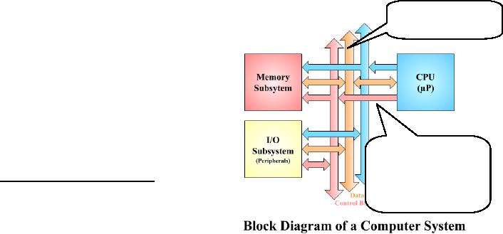
Computer
Bus or
System
Bus
I/O
Buses
The
block diagram of a general
purpose
computer
system that has been
referred to
repeatedly
in this course has three
buses
in
addition to the three most
important
blocks.
These three buses are
collectively
referred
to as the system bus or
the
The bus
interface
computer
bus9. The block
diagram is
unit is
usually
between
the CPU
9
In some
cases, the external CPU
bus is the same as the
system bus, especially in
the case of System bus.
and small,
dedicated
systems. However, for most
systems, there is a "bus
interface unit" between the
CPU and the
system
bus. The bus interface
unit is not shown in the
figure.
Page
242
Last
Modified: 01-Nov-06
Advanced Computer
Architecture-CS501
________________________________________________________
repeated
here for an easy reference in
Figure 1.
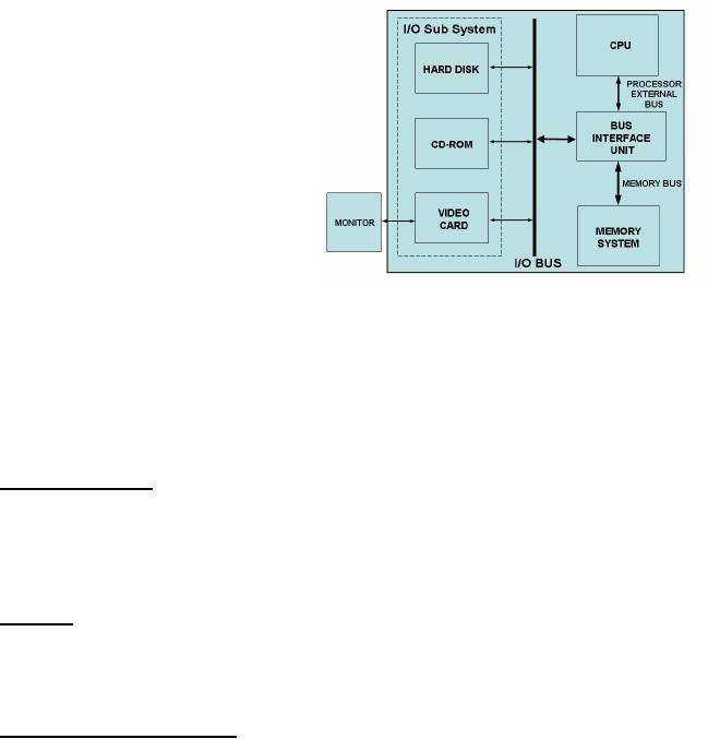
Another
organization that is used in
modern computers is shown in
Figure 2. It has a
memory
bus for connecting the CPU
to the memory subsystem.
This bus
is
separate from the I/O bus
that is used to connect
peripherals and I/O devices to the
Figure
1
system.
Examples
of I/O buses include the PCI
bus and the ISA bus. These I/O
buses provide an
"abstract
interface" that can be used
for interfacing a large
variety of peripherals to
the
system
with minimum hardware. It is also
possible to standardize I/O buses, as done
by
several
agencies, so that third
party manufacturers can build
add-on sub systems for
existing
architectures.
The
location of these I/O buses
may be different in
different
computers.
Earlier
generation computers used
a
single
bus over which the CPU
could
communicate
with the memory as
well
as the
I/O devices. This meant that
the
bandwidth
of the bus was shared
between
the memory and I/O devices.
However,
with the passage of
time,
Figure
1
computer
architects drifted
towards
separate
memory and I/O buses,
thereby
giving more flexibility to
users
wanting
to upgrade their existing
systems.
A main
disadvantage of I/O buses (and
the
buses in general) is that
every bus has a fixed
bandwidth which is shared by
all
Figure
2
devices on
the bus. Additionally,
electrical constraints like
transmission line effects
and
bus
length further reduce the
bandwidth. As a result of this,
the designer has to make a
decision
whether to sacrifice interface
simplicity (by connecting
more devices to the
bus)
at the
cost of bandwidth, or connect fewer
devices to the bus and keep things
simple to
get a
better bandwidth. This can be
explained with the help of
an example.
Example
# 1
Problem
statement:
Consider
an I/O bus that can transfer 4 bytes of
data in one bus cycle. Suppose
that a
designer is
considering to attach the
following two components to
this bus:
Hard
drive, with a transfer rate of 40
Mbytes/sec
Video
card, with a transfer rate of 128
Mbytes/sec.
What will
be the implications?
Solution:
The
maximum frequency of the bus is 30
MHz10. This means
that the maximum
bandwidth
of this bus is 30 x 4 = 120 Mbytes/sec.
Now, the demand for
bandwidth from
these
two components will be 128 + 40 =168
Mbytes/sec which is more
than the 120
10
These
numbers correspond to an I/O
bus that is relatively old. Modern
systems use much faster
buses
than
this.
Page
243
Last
Modified: 01-Nov-06

Advanced Computer
Architecture-CS501
________________________________________________________
Mbytes/sec
that the bus can provide.
Thus, if the designer uses
these two components
with
this bus, one or both of
these components will be operating at
reduced bandwidth.
Bus
arbitration:
Arbitration
is another issue in the use
of I/O buses. Most commercially
available I/O
buses
have protocols defining a
number of things, for
example how many devices
can
access
the bus, what will happen if
multiple devices want to access
the bus at the same
time,
etc. In such situations, an
"arbitration scheme" must be established.
As an example,
in the
SCSI11 specifications,
every device in the system
is assigned an ID which
identifies
the
device to the "bus arbiter".
If multiple devices send a request for
the bus, the
device
with
the highest priority will be
given access to the bus
first. Such a scheme is easy
to
implement
because the arbiter can
easily decide which device
should be given access
to
the
bus, but its disadvantage is
that the device with a
low priority will
not be
able to get access to the bus12. An alternate scheme would
be to give the
highest
priority
to the device that has
been waiting for the
longest time for the
bus. As a result of
this
arbitration, the access
time, or the latency, of
such buses will be further
reduced.
Details
about the PCI and some
other buses will be presented in a
separate section.
Example
# 2
Problem
statement:
If a bus
requires 10 nsec for bus requests, 10
nsec for arbitration and the
average time to
complete
an operation is 15 nsec after
the access to the bus has
been granted, is it
possible
for such a bus to perform 50
million IOPS?
Solution:
For 50
million IOPS, the average
time for each IOP is 1 /
(50 x 106)
=20 nsec. Given
the
information
about the bus, the
sum of the three times is 10
+ 10 + 15 = 35 nsec for a
complete
I/O operation. This means
that the bus can perform a
maximum of 1 / (35 x 10-
9
) = 28.6
million IOPS.
Thus, it
will not be able to perform 50 million
IOPS.
11
Small
Computer System
Interface.
12
Such a
situation is called "starvation".
Page
244
Last
Modified: 01-Nov-06
Table of Contents:
- Computer Architecture, Organization and Design
- Foundations of Computer Architecture, RISC and CISC
- Measures of Performance SRC Features and Instruction Formats
- ISA, Instruction Formats, Coding and Hand Assembly
- Reverse Assembly, SRC in the form of RTL
- RTL to Describe the SRC, Register Transfer using Digital Logic Circuits
- Thinking Process for ISA Design
- Introduction to the ISA of the FALCON-A and Examples
- Behavioral Register Transfer Language for FALCON-A, The EAGLE
- The FALCON-E, Instruction Set Architecture Comparison
- CISC microprocessor:The Motorola MC68000, RISC Architecture:The SPARC
- Design Process, Uni-Bus implementation for the SRC, Structural RTL for the SRC instructions
- Structural RTL Description of the SRC and FALCON-A
- External FALCON-A CPU Interface
- Logic Design for the Uni-bus SRC, Control Signals Generation in SRC
- Control Unit, 2-Bus Implementation of the SRC Data Path
- 3-bus implementation for the SRC, Machine Exceptions, Reset
- SRC Exception Processing Mechanism, Pipelining, Pipeline Design
- Adapting SRC instructions for Pipelined, Control Signals
- SRC, RTL, Data Dependence Distance, Forwarding, Compiler Solution to Hazards
- Data Forwarding Hardware, Superscalar, VLIW Architecture
- Microprogramming, General Microcoded Controller, Horizontal and Vertical Schemes
- I/O Subsystems, Components, Memory Mapped vs Isolated, Serial and Parallel Transfers
- Designing Parallel Input Output Ports, SAD, NUXI, Address Decoder , Delay Interval
- Designing a Parallel Input Port, Memory Mapped Input Output Ports, wrap around, Data Bus Multiplexing
- Programmed Input Output for FALCON-A and SRC
- Programmed Input Output Driver for SRC, Input Output
- Comparison of Interrupt driven Input Output and Polling
- Preparing source files for FALSIM, FALCON-A assembly language techniques
- Nested Interrupts, Interrupt Mask, DMA
- Direct Memory Access - DMA
- Semiconductor Memory vs Hard Disk, Mechanical Delays and Flash Memory
- Hard Drive Technologies
- Arithmetic Logic Shift Unit - ALSU, Radix Conversion, Fixed Point Numbers
- Overflow, Implementations of the adder, Unsigned and Signed Multiplication
- NxN Crossbar Design for Barrel Rotator, IEEE Floating-Point, Addition, Subtraction, Multiplication, Division
- CPU to Memory Interface, Static RAM, One two Dimensional Memory Cells, Matrix and Tree Decoders
- Memory Modules, Read Only Memory, ROM, Cache
- Cache Organization and Functions, Cache Controller Logic, Cache Strategies
- Virtual Memory Organization
- DRAM, Pipelining, Pre-charging and Parallelism, Hit Rate and Miss Rate, Access Time, Cache
- Performance of I/O Subsystems, Server Utilization, Asynchronous I/O and operating system
- Difference between distributed computing and computer networks
- Physical Media, Shared Medium, Switched Medium, Network Topologies, Seven-layer OSI Model