 |
Structural RTL Description of the SRC and FALCON-A |
| << Design Process, Uni-Bus implementation for the SRC, Structural RTL for the SRC instructions |
| External FALCON-A CPU Interface >> |
Advanced Computer
Architecture-CS501
Advanced
Computer Architecture
Lecture
No. 13
Reading
Material
Vincent
P. Heuring & Harry F. Jordan
Chapter
4
Computer
Systems Design and Architecture
4.2.2,
slides
Summary
�
Structural
RTL Description of the SRC
(continued...)
�
Structural
RTL Description of the
FALCON-A
This
lecture is a continuation of the
previous lecture.
Structural
RTL for branch instructions
Let us
take a look at the structural RTL
for branch instructions. We
know that there
are
several
variations of the branch
instructions including unconditional
branch and different
conditional
branches. We look at the RTL for
`branch if zero' (brzr) and
`branch and link
if zero'
brlzr' conditional branches.
The
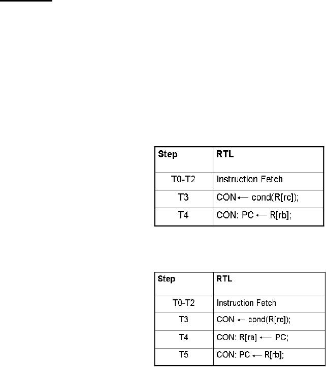
syntax for the branch if
zero (brzr) is:
brzr
rb, rc
As you
may recall, this
instruction
instructs
the processor to branch to
the
instruction
at the address held
in
register
rb, if the value stored
in
register
rc is zero. Time steps for
this
instruction
are outlined in the
table.
The
first three steps are of
the
instruction
fetch phase. Next, the
value
of
register rc is checked and
depending
on the
result, the condition flag
CON is set. In time step
T4, the program counter is
set to
the
register rb value, depending on
the CON bit (the
condition flag).
The
syntax for the branch and
link if zero (brlzr)
is:
brlzr
ra, rb, rc
This
instruction is the same as
the
instruction
brzr
but
additionally the
return
address is saved
(linking
procedure).
The time steps for
this
instruction
are shown in the
table.
Notice
that the steps
for this
instruction
are the same as
the
instruction
brzr with an additional
step
after
the condition bit is set;
the current
Page
158
Last
Modified: 01-Nov-06
Advanced Computer
Architecture-CS501
value of
the program counter is saved
to register ra.
Structural
RTL for shift
instructions
Shift
instructions
are
rather
complicated
in the sense that
they
require
extra hardware to hold
and
decrement
the count. For an
ALSU
that can
perform only single bit
shifts,
the
data must be repeatedly
cycled
through
the ALSU and the
count
decremented
until it reaches zero.
This
approach
presents some
timing
problems,
which can be overcome by
employing
multiple-bit shifts using
a
barrel
shifter.
The
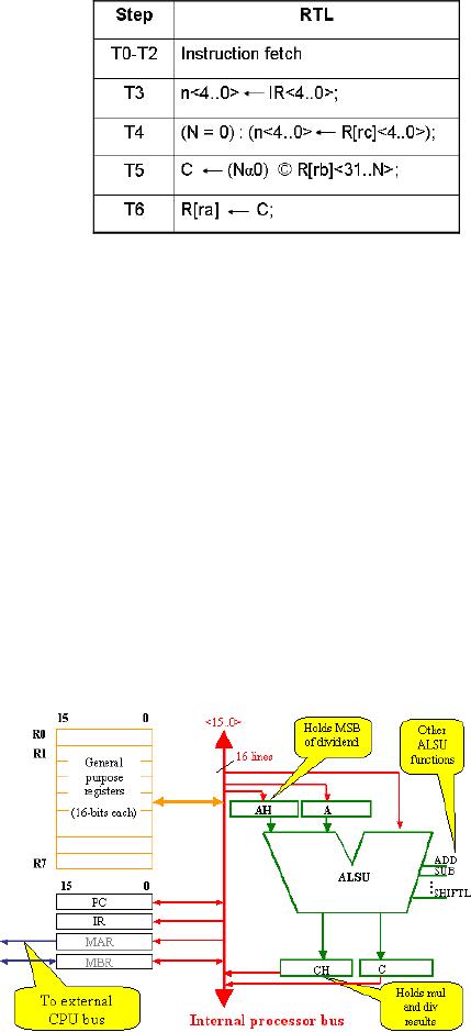
structural RTL for shr
ra, rb, rc or shr
ra, rb, c3 is given
in the corresponding
table
shown. Here n represents a
5-bit register; IR bits 0 to 4
are copied in to it. N is
the
decimal
value of the number in this
register. The actual
shifting is being done in step
T5.
Other
instructions that will have
similar tables are:
shl, shc, shra
e.g.,
for shra, T5 will have C← (NαR [rb]
<31>) R[rb]
<31...N>;
Structural
RTL Description of FALCON-A
Instructions
Uni-bus
data path implementation
Comparing
the uni-bus implementation of FALCON-A
with that of SRC results in
the
following
differences:
�
FALCON-A
processor bus has 16 lines
or is 16-bits wide while that of SRC
is
32-bits
wide.
� All registers of
FALCON-A are of 16-bits
while in case of SRC all registers
are
32-bits.
� Number
of registers in FALCON-A are 8 while in
SRC the number of registers is
32.
� Special
registers i.e. Program Counter
(PC) and Instruction Register
(IR) are 16-
bit
registers while
in SRC
these are
32-bits.
� Memory
Address
Register
(MAR)
and
Memory Buffer
Register
(MBR) are
also of
16-bits
while in
SRC these
are of
32-bits.
MAR and MBR
are dual
port
registers. At one side
they
are connected to
internal
bus and at other
Page
159
Last
Modified: 01-Nov-06
Advanced Computer
Architecture-CS501
side to
external memory in order to
point to a particular address
for reading or
writing
data
from or to the memory and MBR
would get the data from
the memory.
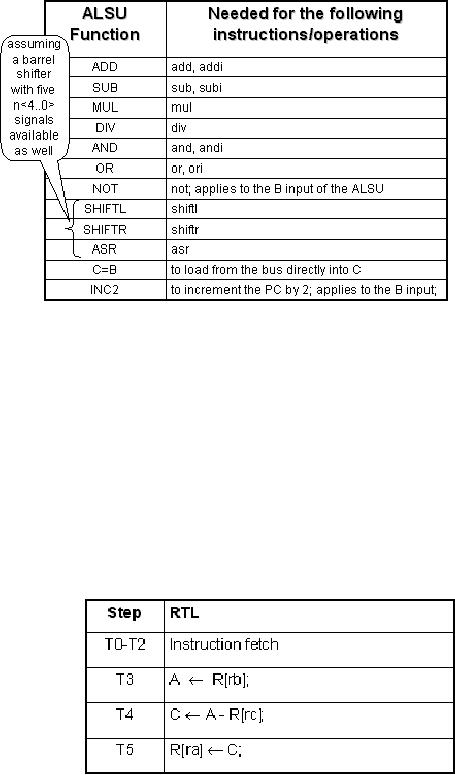
ALSU
functions needed
ALSU of
FALCON-A has slightly
different functions. These functions
are given in the
table.
Note
that mul
and
div
are
two significant
instructions
in this
instruction
set. So
whenever
one of these
instructions
is activated,
the
ALSU unit would
take the
operand from
its
input and provide the
output
immediately, if
we
neglect the
propagation
delays to
its
output. In case of
FACON-A,
we have
two
registers A and AH
each of
16-bits. AH
would
contain the
higher
16-bits or most significant
16-bits of a 32-bit operand. This
means that the
ALSU
provides
the facility of using 32-bit
operand in certain instructions. At the
output of
ALSU we
could have a 32-bit result
and that can not be saved in
just one register C so we
need to
have another one that is CH.
CH can store the most significant
16-bits of the
result.
Why
do we need to add AH and CH?
This is
because we have mul and div
instructions in the instruction
set of the FALCON-
A. So for
that case, we can implement
the div instruction in
which, at the input, one of
the
operand
which is dividend would be
32-bits or in case of mul
instruction the
output
which is
the result of multiplication of
two 16-bit numbers, would be
32-bit that could be
placed in C and
CH. The data in these 2
registers will be concatenated and so would be
the
input operand in two registers AH and A.
Conceptually one could consider
the A and
AH
together to represent 32-bit
operand.
Structural
RTL for subtract
instruction
sub
ra, rb, rc
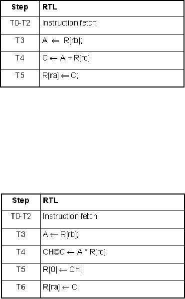
In sub
instruction three registers
are
involved.
The first three steps
will
fetch
the sub instruction and in
T3,
T4, T5
the steps for execution
of
the sub
instruction will be
performed.
Page
160
Last
Modified: 01-Nov-06
Advanced Computer
Architecture-CS501
Structural
RTL for addition
instruction
add
ra, rb, rc
The
table of add instruction
is
almost
same as of sub instruction
except in
timing step T4 we have
+
sign
for addition instead of
sign
as in sub
instruction. Other instructions
that belong to the same
group are `and', `or'
and
`sub'.
Structural
RTL for multiplication
instruction
mul
ra, rb, rc
This
instruction is only present in this
processor and not in SRC.
The first three steps
are
exactly
same as of other
instructions
and would fetch the
mul
instruction. In step T3 we will
bring
the contents of register R
[rb]
in the
buffer register A at the
input
of ALSU.
In step T4 we take the
multiplication
of A with the contents of
R[rc] and put it at the
output of the ALSU in
two
registers C and
CH. CH would contain the
higher 16-bits while
register C would
contain
the
lower 16-bits. Now these
two registers cannot transfer
the data in one bus cycle to
the
registers, since
the width is 16-bits. So we
need to have 2 timing steps,
in T5 we transfer
the
higher byte to register R[0]
and in T6 the lower 16-bits
are transferred to
the
placeholder
R[a]. As a result of multiplication
instruction we need 3 timing
steps for
Instruction
Fetch and 4 timing steps for
Instruction Execution and 7 steps
altogether.
Structural
RTL for division
instruction
Page
161
Last
Modified: 01-Nov-06
Advanced Computer
Architecture-CS501
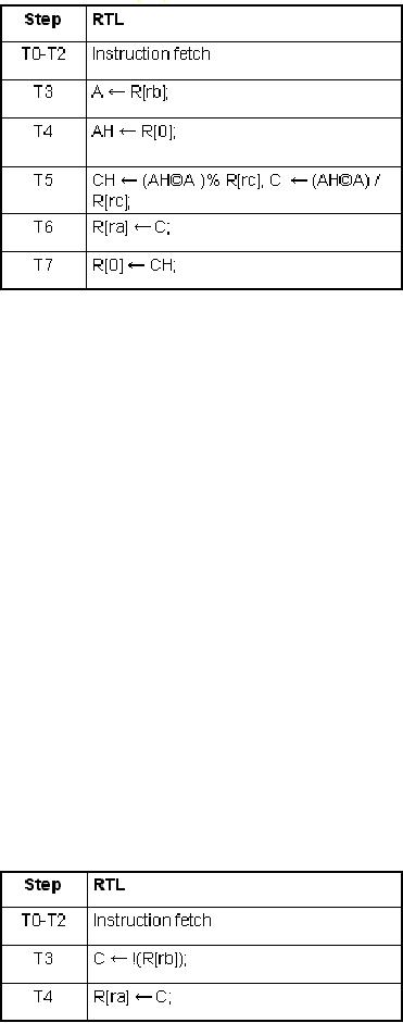
div
ra, rb, rc
In this
instruction first three
steps
are
the same. In step T3
the
contents
of register rb are placed in
buffer
register A and in step T4 we
take the
contents of register R[0]
in
to the
register AH. We assume
before
using the divide instruction
that we will place the higher
16-bits of dividend to
register
R[0]. Now in T5 the actual
division takes place in two
concurrent operations. We
have
the dividend at the input of
ALSU unit represented by
concatenation of AH and A.
Now as a
result of division instruction,
the first operation would
take the remainder.
This
means
divide AH concatenated with A with
the contents given in
register rc and the
remainder
is placed in register CH at the output of
ALSU. The quotient is placed in C.
In
T6 we take C to
the register R[ra] and in T7
remainder available in CH is taken to
the
default
register R[0] through the
bus. In divide instruction 5
timing steps are required
to
execute
the instruction while 3 to
fetch the
instruction.
Note:
Corresponding to mul and div
instruction one should be careful
about the
additional
register R[0] that it should
be properly loaded prior to use
the instructions e.g.
if in the
divide instruction we don't
have the appropriate data
available in R[0] the
result
of divide
instruction would be
wrong.
Structural
RTL for not
instruction
not
ra, rb
In this
instruction first three
steps
will
fetch the instruction. In T3
we
perform
the not operation
of
contents
in R[rb] and transfer
them
in to the
buffer register C. It is
simply
the one's
complement
changing
of 0's to 1's and 1's
to
0's. In
timing step T4 we take
the
contents
of register C and transfer to register
R[ra] through the bus as
shown in its
corresponding
table.
Page
162
Last
Modified: 01-Nov-06
Advanced Computer
Architecture-CS501
Structural
RTL for add immediate
instruction
addi
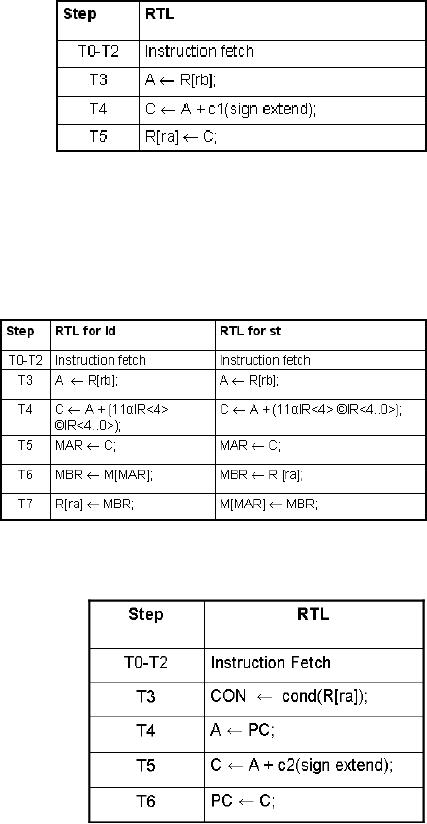
ra, rb, c1
In this
instruction c1 is a constant as a part of
the instrucion. First three
steps are for
Instruction
Fetch operation. In T3
we take
the contents of register
R
[rb] in
to the buffer register A.
In
T4 we add
up the contents of A
with
the constant c1 after
sign
extension
and bring it to C.
Sign
extension of 5-bit c1 and
8-bit
constant c2
Sign
extension for 5-bit c1 is:
(11αIR<4>
�IR<4.. 0>)
We have
immediate constant c1 in the
form of lower 5-bits and bit
number 4 indicates
the
sign
bit. We just copy it to the
left most 11 positions to make it a
16-bit number.
Sign
extension for 8-bit c2
is:
(8αIR<7>
�IR<7.. 0>)
In the
same way for constant c2 we
need to place the sign bit
to the left most 8 position
to
make it
16-bit number.
Structural
RTL for the load
and store
instruction
Tables
for load and store
instructions
are same as
SRC
except a slight
difference
in the notation.
So when
we have square
brackets [R
[rb]+c1], it
corresponds to
the base
address
in R[rb] and an offset taken
from c1.
Structural
RTL for conditional jump
instructions
jz
ra, [c2]
In first
three steps of this table,
the
instruction
is fetched. In T3 we set a 1-
bit
register "CON" to true if
the
condition
is met.
How
do we test the condition?
This is
tested by the contents given
by
the
register ra. So condition
within
square
brackets is R[ra]. This
means
test the
data given in register ra.
There
are
different possibilities and so the
data could be positive,
negative or zero. For
this
particular
instruction it would be tested if
the data were zero. If
the data were zero,
the
"CON"
would be 1.
Page
163
Last
Modified: 01-Nov-06
Advanced Computer
Architecture-CS501
In T4 we
just take the contents of
the PC into the buffer
register A. In T5 we add up
the
contents
of A to the constant c2 after
sign extension. This
addition will give us
the
effective
address to which a jump
would be taken. In T6, this
value is copied to the
PC.
In
FALCON-A, the number of
conditional jumps is more
than in SRC. Some of
which
are
shown below:
� jz
(op-code= 19) jump
if zero
jz r3,
[4]
(R[3]=0):
PC←
PC+
2;
� jnz
(op-code= 18) jump
if not zero
jnz
r4, [variable]
(R[4]≠0):
PC←
PC+
variable;
� jpl
(op-code= 16) jump
if positive
jpl
r3, [label]
(R[3]≥0): PC
←
PC+
(label-PC);
� jmi
(op-code= 17) jump
if negative
jmi
r7, [address]
(R[7]<0):
PC←
PC+
address;
The
unconditional jump instruction will be
explained in the next
lecture.
Page
164
Last
Modified: 01-Nov-06
Table of Contents:
- Computer Architecture, Organization and Design
- Foundations of Computer Architecture, RISC and CISC
- Measures of Performance SRC Features and Instruction Formats
- ISA, Instruction Formats, Coding and Hand Assembly
- Reverse Assembly, SRC in the form of RTL
- RTL to Describe the SRC, Register Transfer using Digital Logic Circuits
- Thinking Process for ISA Design
- Introduction to the ISA of the FALCON-A and Examples
- Behavioral Register Transfer Language for FALCON-A, The EAGLE
- The FALCON-E, Instruction Set Architecture Comparison
- CISC microprocessor:The Motorola MC68000, RISC Architecture:The SPARC
- Design Process, Uni-Bus implementation for the SRC, Structural RTL for the SRC instructions
- Structural RTL Description of the SRC and FALCON-A
- External FALCON-A CPU Interface
- Logic Design for the Uni-bus SRC, Control Signals Generation in SRC
- Control Unit, 2-Bus Implementation of the SRC Data Path
- 3-bus implementation for the SRC, Machine Exceptions, Reset
- SRC Exception Processing Mechanism, Pipelining, Pipeline Design
- Adapting SRC instructions for Pipelined, Control Signals
- SRC, RTL, Data Dependence Distance, Forwarding, Compiler Solution to Hazards
- Data Forwarding Hardware, Superscalar, VLIW Architecture
- Microprogramming, General Microcoded Controller, Horizontal and Vertical Schemes
- I/O Subsystems, Components, Memory Mapped vs Isolated, Serial and Parallel Transfers
- Designing Parallel Input Output Ports, SAD, NUXI, Address Decoder , Delay Interval
- Designing a Parallel Input Port, Memory Mapped Input Output Ports, wrap around, Data Bus Multiplexing
- Programmed Input Output for FALCON-A and SRC
- Programmed Input Output Driver for SRC, Input Output
- Comparison of Interrupt driven Input Output and Polling
- Preparing source files for FALSIM, FALCON-A assembly language techniques
- Nested Interrupts, Interrupt Mask, DMA
- Direct Memory Access - DMA
- Semiconductor Memory vs Hard Disk, Mechanical Delays and Flash Memory
- Hard Drive Technologies
- Arithmetic Logic Shift Unit - ALSU, Radix Conversion, Fixed Point Numbers
- Overflow, Implementations of the adder, Unsigned and Signed Multiplication
- NxN Crossbar Design for Barrel Rotator, IEEE Floating-Point, Addition, Subtraction, Multiplication, Division
- CPU to Memory Interface, Static RAM, One two Dimensional Memory Cells, Matrix and Tree Decoders
- Memory Modules, Read Only Memory, ROM, Cache
- Cache Organization and Functions, Cache Controller Logic, Cache Strategies
- Virtual Memory Organization
- DRAM, Pipelining, Pre-charging and Parallelism, Hit Rate and Miss Rate, Access Time, Cache
- Performance of I/O Subsystems, Server Utilization, Asynchronous I/O and operating system
- Difference between distributed computing and computer networks
- Physical Media, Shared Medium, Switched Medium, Network Topologies, Seven-layer OSI Model