 |
2-INPUT 4-BIT MULTIPLEXER, 8, 16-Input Multiplexer, Logic Function Generator |
| << BCD to 7-Segment Decoder, Decimal-to-BCD Encoder |
| Applications of Demultiplexer, PROM, PLA, PAL, GAL >> |
CS302 -
Digital Logic & Design
Lesson
No. 18
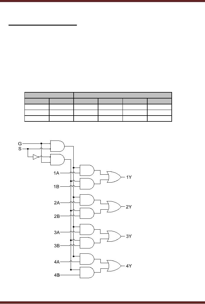
a) 2-INPUT
4-BIT MULTIPLEXER
The
MSI, 74X157 is a 2-input,
4-bit Multiplexer. This
multiplexer has two sets of
4-bit
inputs. It
also has 4-bit outputs.
The single select input
line allows the first
set of four inputs or
the
second set of 4-inputs to be
connected to the output.
Thus four-bits of data from
two
sources
are routed to the output.
The function table and
the circuit of the
multiplexer are
shown.
table 18.1, figure
18.1
The
multiplexer has two sets of
4-bit active-high inputs 1A,
2A, 3A, 4A and 1B,
2B, 3B,
4B respectively.
The multiplexer has 4-bit
active-high outputs 1Y, 2Y,
3Y 4Y. The single
select
input
allows either the 4-bit
input A or the 4-bit input B
to be connected to the 4-bit
output Y.
The G
active-low pin enables or
disables the
Multiplexer.
Inputs
Outputs
G
S
1Y
2Y
3Y
4Y
1
X
0
0
0
0
0
0
1A
2A
3A
4A
0
1
1B
2B
3B
4B
Table
18.1
Function
table of 2-Input 4-Bit
Multiplexer
Figure
18.1
2-input
4-bit Multiplexer
169
CS302 -
Digital Logic & Design
Expanding
Multiplexers
Multiplexers
have to be connected together to
form larger multiplexer to
fulfil specific
application
requirements.
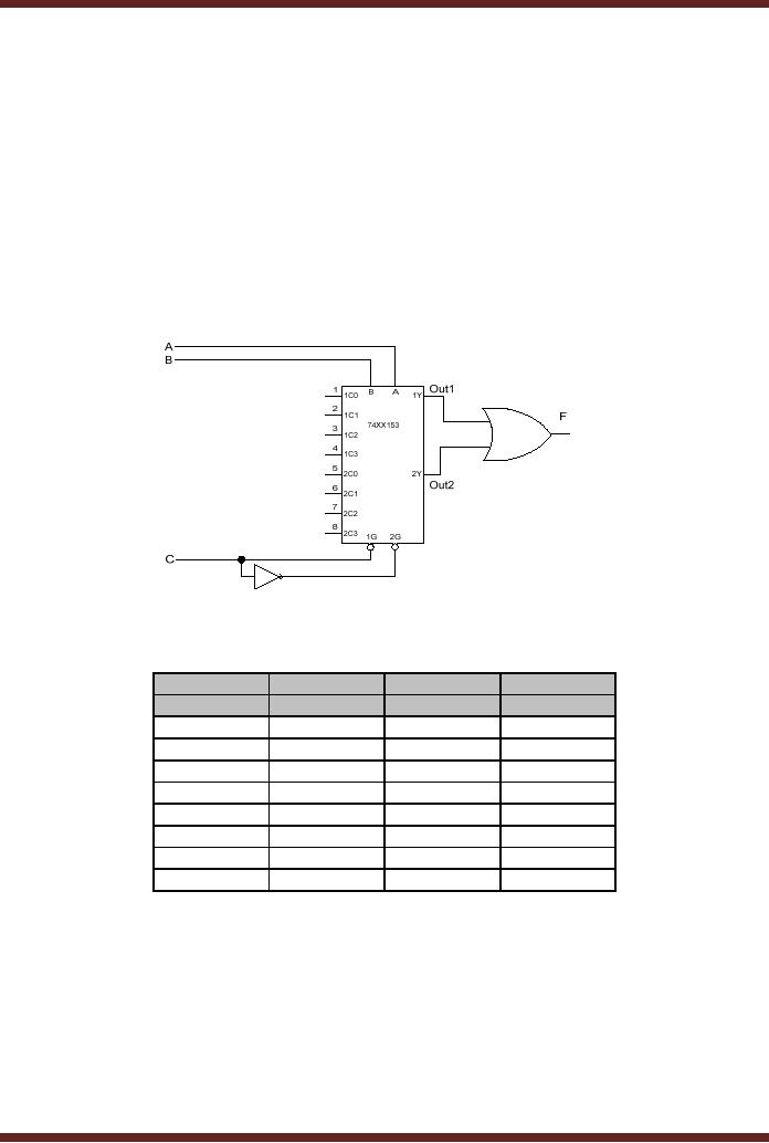
1. 8-Input
Multiplexer
A single
dual, 4-input multiplexer
74X153 can be connected to
form an 8-input
multiplexer.
The circuit diagram and
the function table are
shown in fig. 18.2 and
table 18.2
respectively.
The two active-low enable
inputs of the two 4-input
multiplexers are
connected
together
using a NOT gate to form
the C input of the 8-input
multiplexer. When C is set to
0,
the
first multiplexer is selected
allowing its inputs 1C0,
1C1, 1C2 and 1C3 to be
selected
through
select inputs A and B. When
C is set to 1, the second
multiplexer is selected
allowing
its
inputs and outputs to be
used. The two outputs
are connected through an OR
gate.
Figure
18.2
8-to-1
Multiplexer using two 4-to-1
Multiplexers
Input
Output
C
B
A
F
0
0
0
1C0
0
0
1
1C1
0
1
0
1C2
0
1
1
1C3
1
0
0
2C0
1
0
1
2C1
1
1
0
2C2
1
1
1
2C3
Table
18.2
Function
Table of a 8-to-1
Multiplexer
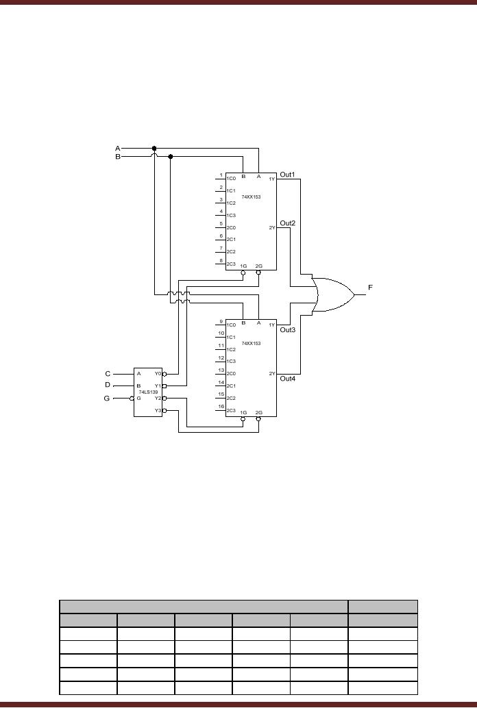
2. 16-Input
Multiplexer
Two
74XX153 Dual, 4-input
multiplexer can be connected to
form a 16-input
multiplexer.
The circuit diagram and
the function table of the 16
input multiplexer are shown
in
Figure
18.3 and table 18.3
respectively.
170
CS302 -
Digital Logic & Design
The
select inputs A and B of the
two dual, 4-input
multiplexers are connected
together
which
allows selection of any one
input out of the four
set of 4-bit inputs. The
four active-low
multiplexer
enable inputs which allow
selection of any one of the
four multiplexers are
connected to
the active-low outputs of a
2-to-4 decoder. The decoder
inputs C and D enable
one
out of the four
multiplexers. The four
outputs are connected
together through a
4-input
OR gate.
The G enable input of the
decoder when set to 1
disables the decoder and
the
multiplexers.
Figure
18.3
16-input
Multiplexer
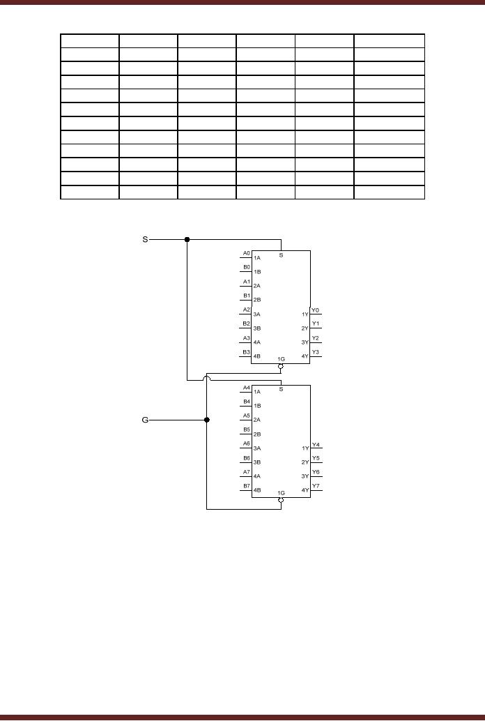
3. 2-Input,
8-bit Multiplexer
Two
2-input, 4-bit multiplexers
74X157 can be connected to
implement a 2-input,
8-bit
multiplexer.
The circuit diagram is shown
in figure 18.4. The select S
inputs of the two
multiplexers
are connected together so
that the 4-bit inputs A of
both the multiplexers
are
selected
simultaneously when S is set to
logic low. Similarly, by
setting the S input to
logic-
high
the B inputs of both the
multiplexers are selected.
The active-low enable inputs
G of both
the
multiplexers are also
connected together so that
both the multiplexers are
enabled and
disabled
simultaneously by setting the G
input to 0 or 1 respectively.
Inputs
Output
G
D
C
B
A
F
1
x
x
x
x
0
0
0
0
0
0
1C0
(M1)
0
0
0
0
1
1C1
(M1)
0
0
0
1
0
1C2
(M1)
0
0
0
1
1
1C3
(M1)
171
CS302 -
Digital Logic & Design
0
0
1
0
0
2C0
(M1)
0
0
1
0
1
2C1
(M1)
0
0
1
1
0
2C2
(M1)
0
0
1
1
1
2C3
(M1)
0
1
0
0
0
1C0
(M2)
0
1
0
0
1
1C1
(M2)
0
1
0
1
0
1C2
(M2)
0
1
0
1
1
1C3
(M2)
0
1
1
0
0
2C0
(M2)
0
1
1
0
1
2C1
(M2)
0
1
1
1
0
2C2
(M2)
0
1
1
1
1
2C3
(M2)
Table
18.3
Function
Table of 16-bit
Multiplex
Figure
18.4 2-Input, 8-bit
Multiplexer
Applications of
Multiplexers
Multiplexers
are used in a wide variety
of applications. Their primary
use is to route
data
from multiple sources to a
single destination. Other
than its use as a Data
router, a
parallel to
serial converter, logic
function generator and used
for operation
sequencing.
1. Data
Routing
A two
digit 7-Segment display uses
two 7-Segments Display
digits connected to
two
BCD to
7-Segment display circuits. To
display the number 29 the
BCD number 0010
representing
the MSD is applied at the
inputs of the BCD to
7-Segment display
circuit
connected to
the MSD 7-Segment Display
Digit. Similarly, the BCD
input 1001
representing
the
numbers 9 is applied at the
inputs of the LSD display
circuit. The circuit uses
two BCD to
7-Segment
decoder circuits to decode
each of the two BCD
inputs to the respective
7-
172
CS302 -
Digital Logic & Design
Segment
display outputs. Figure
18.5. The display circuit
can be implemented using a
single
BCD to
7-Segment IC and a
Multiplexer.
Figure
18.5
2-Digit
Decimal Display
Circuit
To fully
understand the working of
the alternate circuit it is
essential to understand
the
working of
the 7-Segment Display Digit.
7-Segment Display Digits are
implemented using 7
LEDs
(Light Emitting Diodes)
connected in the form of
number 8. To turn on a LED,
its Anode
is connected to
+5 volts and its Cathode is
connected to Ground or 0 volts.
7-Segment
displays
are of two types, the
Common Anode type and
the Common Cathode
type.
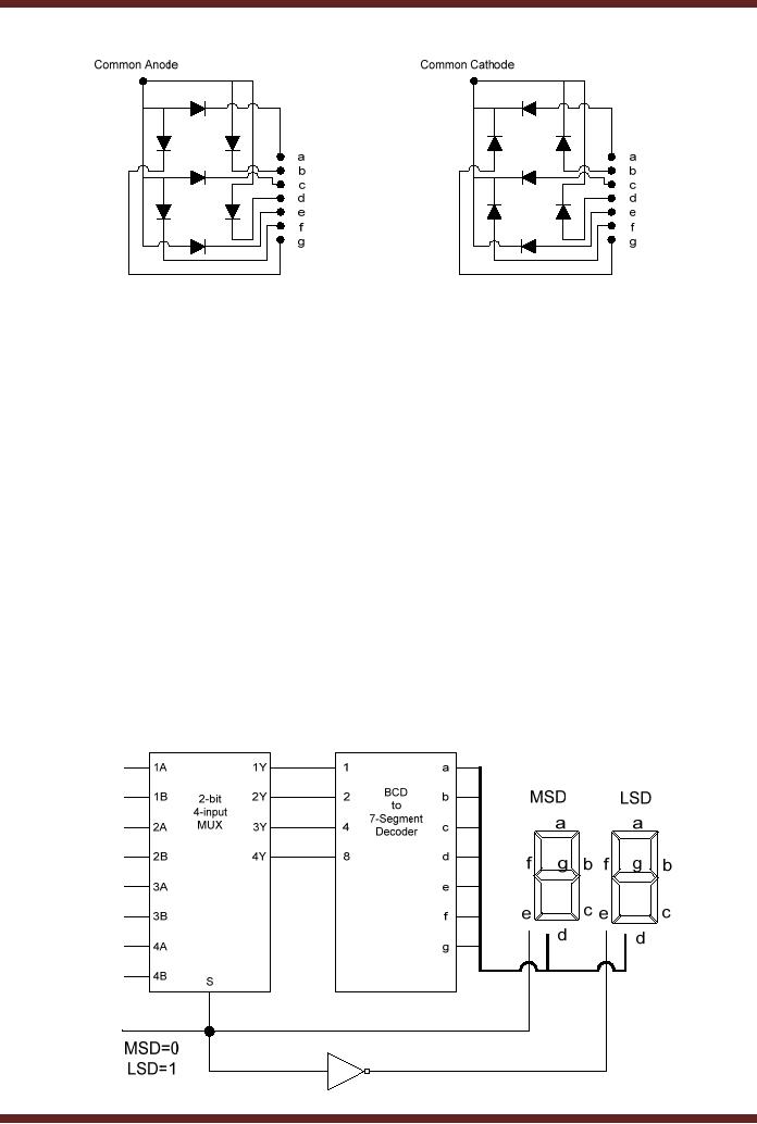
a. Common
Anode 7-Segment
Display
The
Common Anode 7-Segment
Display has positive end of
each of the seven
display
segments
(LEDs) connected together. To
display any segment the
Common Anode of the
display
has to be connected to +5 volts
and the other end of
each segment has to
be
connected to 0
volts. Figure 18.6a
b. Common
Cathode 7-Segment
Display
The
Common Cathode 7-Segment
Display has negative end of
each of the seven
display
segments (LEDs) connected
together. To display any
segment the Common
Cathode
of the
display has to be connected to 0
volts and the other
end of each segment has to
be
connected to +5
volts. Figure 18.6b.
173
CS302 -
Digital Logic & Design
Figure
18.6
Common
Anode and Common Cathode
7-Segment Displays
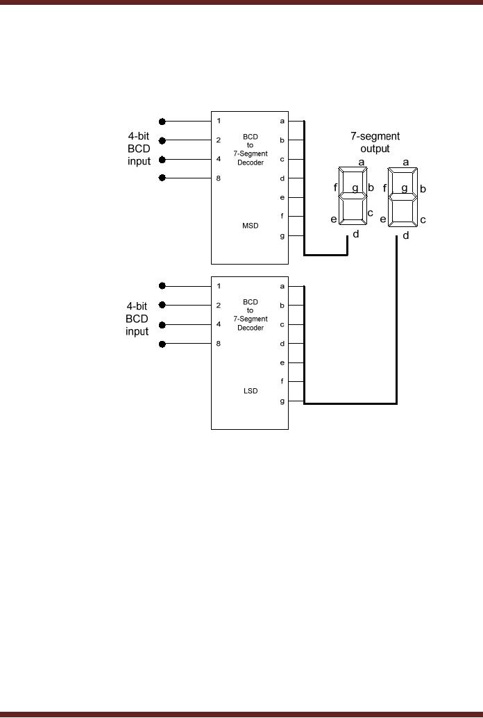
The
alternate 2-digit display
circuit based on a multiplexer
and a BCD to
7-Segment
Decoder is
shown in figure 18.7. The
BCD numbers of the two
digits to be displayed
are
applied at
the inputs A and B of the
multiplexer. The 4-bit
output of the Multiplexer
is
connected to
the 4-bit input of the
BCD to 7-Segment Decoder
circuit. The 7-Segment
output
of the
Decoder is connected to the 7
segments of both the Common
Cathode Displays. The
MSD/LSD
input is connected to the
select input of the
Multiplexer, the Common
Cathode of
the MSD
and the Common Cathode of
the LSD through a NOT
gate. The MSD is applied
at
Input A,
and the LSD at input B. To
Display the MSD the MSD/LSD
input is set to 0. The
BCD
number at
Input A of the multiplexer is
selected and routed through
the BCD to 7-Segment
Decoder to
both the two 7-Segment
Displays. Since the MSD/LSD
input is 0 therefore
the
MSD display is
selected and the MSD is
displayed. The MSD/LSD input
is switched to 1,
which
selects the BCD at input B
which is routed through the
Multiplexer to the
7-Segment
Decoder
and ultimately to the
7-segment displays. Since
the MSD/LSD is set to 1,
the
Common
Cathode of the LSD is
connected to zero, thus the
number at input B of
the
multiplexer is
displayed on the LSD
display. The MSD/LSD input
is rapidly switched between
0
and 1 to
allow both the digits to be
seen on the 2-digit display.
This circuit can be expanded
to
incorporate
any number of digits.
174
CS302 -
Digital Logic & Design
Figure
18.7
2-Digit
Decimal Display using a
Multiplexer
2. Parallel to
Series Conversion
In a Digital
System, Binary data is used
and represented in parallel.
Parallel data is a
set of
multiple bits. For example,
a nibble is a parallel set of
4-bits, a byte is a parallel
set of 8
bits.
When two binary numbers
are added, the two
numbers are represented in
parallel and
the
parallel adder works and
generates a sum term which
is also in parallel.
Transmission of
information to remote locations
through a piece of wire
requires that
the
parallel information (data) be
converted into serial form.
In a serial data
representation,
data is
represented by a sequence of single
bits. An 8-bit parallel data
can be transmitted
through a
single piece of wire 1-bit
at a time. Transmitting 8-bits
simultaneously (in
parallel
form)
requires 8 separate wires
for the 8-bits. Laying of 8
wires across two remote
locations for
data
transfer is expensive and is
therefore not practical. All
communication systems set
up
across
remote locations use serial
transmission.
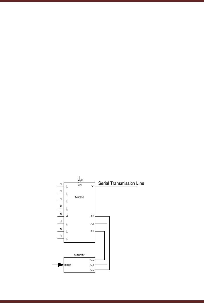
An 8-bit
parallel data can be
converted into serial data
by using an 8-to-1
multiplexer
such as
74X151 which has 8 inputs
and a single output. The
8-bit data which is to
be
transmitted
serially is applied at the 8
inputs I0-7 of the multiplexer. A three
bit counter which
counts
from 0 to 7 is connected to the
three select inputs S0, S1 and S2. The counter is
connected to a
clock which sends a clock
pulse to the counter every 1
millisecond. Initially,
the
counter is
reset to 000, the I0 input is selected and
the data at input I0 is routed to the output
of
the
multiplexer. On receiving the
clock signal after 1
millisecond the counter
increments its
count
from 000 to 001 which
selects I1
input of
the multiplexer and routes
the data present at
the
input to the output.
Similarly, at the next clock
pulse the counter increments
to 010,
selecting
I2 input and
routing the data to the
output. Thus after 8
milliseconds the parallel
data
is routed to
the output 1-bit at a time.
The output of the
multiplexer is connected to the
wire
through
which the serial data is
transmitted. Figure
18.8
Figure
18.8a
Parallel to
Serial Conversion
175
CS302 -
Digital Logic & Design
0
1
2
3
4
5
6
7
C0
C1
C2
Y
Figure
18.8b Timing diagram of the
Parallel to Serial Conversion
Circuit
3. Logic
Function Generator
Multiplexers
can be used to implement a
logic function directly from
the function table
without
the need for simplification.
The select inputs of the
multiplexer are used as the
function
variables.
The inputs of the
multiplexer are connected to
logic 1 and 0 to represent
the missing
and
available terms. The three
variable function table and
its 8-to-1 multiplexer based
function
implementation
is shown in figure
18.9
Input
Output
A
B
C
Y
0
0
0
1
0
0
1
1
0
1
0
1
0
1
1
0
1
0
0
0
1
0
1
1
1
1
0
0
1
1
1
1
Figure
18.9
Logic
Function Generator based on
3-variable logic function
table
4. Operation
Sequencing
Many industrial
applications have processes
that run in a sequence. A
paint
manufacturing
plant might have a four
step process to manufacture
paint. Each of the
four
steps
runs in a sequence one after
the other. The second
step can not start
before the first
step
has completed. Similarly,
the third and fourth
step of the paint
manufacturing process
can
not
proceed unless steps two
and three have completed. It
is not necessary that each
of the
manufacturing
steps is of the same
duration. Each manufacturing
step can have different
time
176
CS302 -
Digital Logic & Design
duration
and can be variable
depending upon the quantity
of paint manufactured or
other
parameters.
Normally, the end of each
step in the manufacturing
process is indicated by a
signal
which is actuated by some
machine which has completed
its part of the
manufacturing
process. On
receiving the signal the
next step of the
manufacturing process is
initiated.
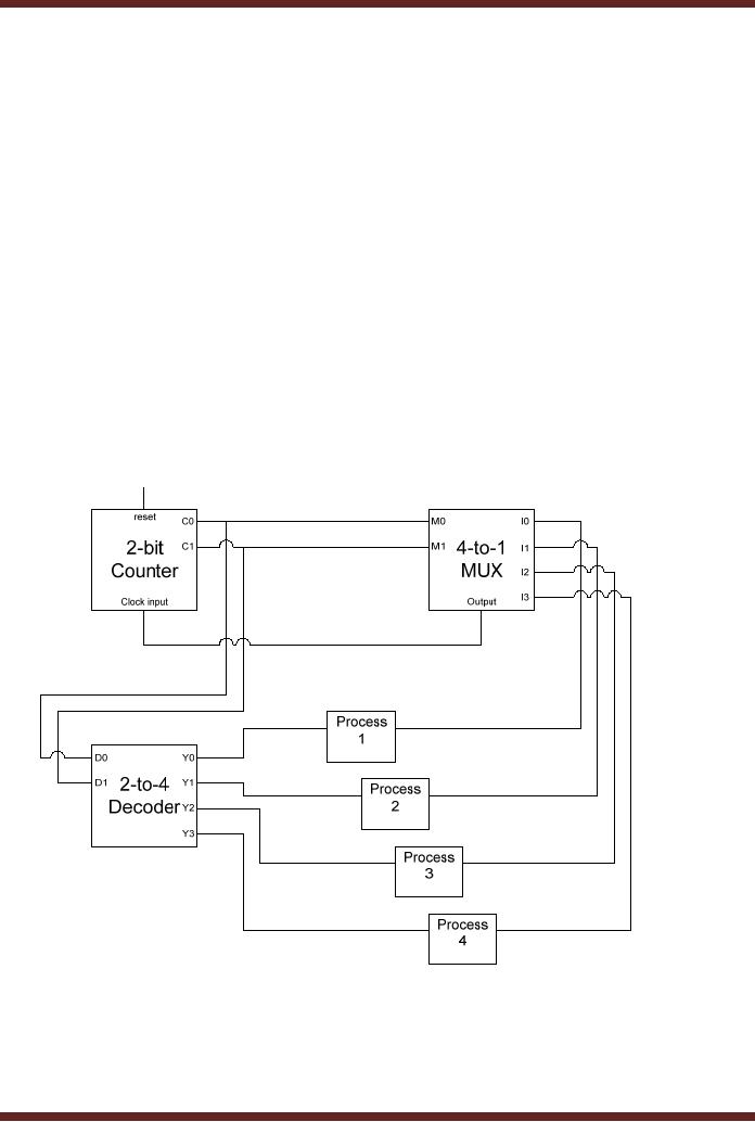
The
entire sequence of operations is
controlled by a Multiplexer and a
Decoder circuit.
Figure
18.10. The manufacturing
processes are started by
resetting the 2-bit counter
to 00.
The
counter output is connected to
the select input of the
Multiplexer and the inputs
of the
Decoder
which selects the
Multiplexer input I0 is and
activates the Decoder output
Y0. The
Decoder
output is connected to initiate
the first process. When
the process completes
it
indicates
the completion of the
process by setting its
output to logic 1. The
output of Process 1
is connected to
I0 input of the Multiplexer.
When Process 1 sets its
output to 1 to indicate
its
completion,
the logic 1 is routed by the
Multiplexer to the clock
input of the 2-it counter.
The
counter on
receiving logic 1 increments
its count to 01, which
selects I1 input of the
Multiplexer
and
the Y1 output of the
Decoder. The input to
Process 1 is deactivated and
Process 2 is
activated by
Y1. On completion of Process 2
its output is set to logic
1, which is routed by
the
multiplexer to
the clock input of the
2-bit counter which
increments to the next
count. This
continues
until Process 4 signals its
completion after which the
Decoder and the Multiplexer
is
deselected
completing the manufacturing
process.
Figure
18.10
Control of
Manufacturing process through
Operation Sequencing
177
Table of Contents:
- AN OVERVIEW & NUMBER SYSTEMS
- Binary to Decimal to Binary conversion, Binary Arithmetic, 1s & 2s complement
- Range of Numbers and Overflow, Floating-Point, Hexadecimal Numbers
- Octal Numbers, Octal to Binary Decimal to Octal Conversion
- LOGIC GATES: AND Gate, OR Gate, NOT Gate, NAND Gate
- AND OR NAND XOR XNOR Gate Implementation and Applications
- DC Supply Voltage, TTL Logic Levels, Noise Margin, Power Dissipation
- Boolean Addition, Multiplication, Commutative Law, Associative Law, Distributive Law, Demorgans Theorems
- Simplification of Boolean Expression, Standard POS form, Minterms and Maxterms
- KARNAUGH MAP, Mapping a non-standard SOP Expression
- Converting between POS and SOP using the K-map
- COMPARATOR: Quine-McCluskey Simplification Method
- ODD-PRIME NUMBER DETECTOR, Combinational Circuit Implementation
- IMPLEMENTATION OF AN ODD-PARITY GENERATOR CIRCUIT
- BCD ADDER: 2-digit BCD Adder, A 4-bit Adder Subtracter Unit
- 16-BIT ALU, MSI 4-bit Comparator, Decoders
- BCD to 7-Segment Decoder, Decimal-to-BCD Encoder
- 2-INPUT 4-BIT MULTIPLEXER, 8, 16-Input Multiplexer, Logic Function Generator
- Applications of Demultiplexer, PROM, PLA, PAL, GAL
- OLMC Combinational Mode, Tri-State Buffers, The GAL16V8, Introduction to ABEL
- OLMC for GAL16V8, Tri-state Buffer and OLMC output pin
- Implementation of Quad MUX, Latches and Flip-Flops
- APPLICATION OF S-R LATCH, Edge-Triggered D Flip-Flop, J-K Flip-flop
- Data Storage using D-flip-flop, Synchronizing Asynchronous inputs using D flip-flop
- Dual Positive-Edge triggered D flip-flop, J-K flip-flop, Master-Slave Flip-Flops
- THE 555 TIMER: Race Conditions, Asynchronous, Ripple Counters
- Down Counter with truncated sequence, 4-bit Synchronous Decade Counter
- Mod-n Synchronous Counter, Cascading Counters, Up-Down Counter
- Integrated Circuit Up Down Decade Counter Design and Applications
- DIGITAL CLOCK: Clocked Synchronous State Machines
- NEXT-STATE TABLE: Flip-flop Transition Table, Karnaugh Maps
- D FLIP-FLOP BASED IMPLEMENTATION
- Moore Machine State Diagram, Mealy Machine State Diagram, Karnaugh Maps
- SHIFT REGISTERS: Serial In/Shift Left,Right/Serial Out Operation
- APPLICATIONS OF SHIFT REGISTERS: Serial-to-Parallel Converter
- Elevator Control System: Elevator State Diagram, State Table, Input and Output Signals, Input Latches
- Traffic Signal Control System: Switching of Traffic Lights, Inputs and Outputs, State Machine
- Traffic Signal Control System: EQUATION DEFINITION
- Memory Organization, Capacity, Density, Signals and Basic Operations, Read, Write, Address, data Signals
- Memory Read, Write Cycle, Synchronous Burst SRAM, Dynamic RAM
- Burst, Distributed Refresh, Types of DRAMs, ROM Read-Only Memory, Mask ROM
- First In-First Out (FIFO) Memory
- LAST IN-FIRST OUT (LIFO) MEMORY
- THE LOGIC BLOCK: Analogue to Digital Conversion, Logic Element, Look-Up Table
- SUCCESSIVE APPROXIMATION ANALOGUE TO DIGITAL CONVERTER